Method for manufacturing solid-state imaging device

a solid-state imaging and manufacturing method technology, applied in the direction of color television, television systems, radio control devices, etc., can solve the problems of reducing the capability of readout by the transfer gate, limiting the forming of shallow, heavily doped p-type semiconductor regions by ion implantation, and difficult low-temperature processes, so as to achieve the effect of suppressing the dark current attributed to the interface sta

Inactive Publication Date: 2009-08-20
SONY CORP
View PDF1 Cites 21 Cited by
  • Summary
  • Abstract
  • Description
  • Claims
  • Application Information

AI Technical Summary

Benefits of technology

[0026]Due to the forming of the negative-charge accumulated layer having negative fixed charges above the detection plane of the charge generator, a HAD structure for turning the surface of the charge generator into the hole accumulated state can be achieved, which allows suppression of dark current components attribute...

Problems solved by technology

Therefore, it is difficult for a low-temperature process with temperatures of 400° C. or lower to form the p-type semiconductor region by ion implantation.
Furthermore, in the manufacturing method of Patent Document 1, there is a limit to the forming of the shallow, heavily-doped p-type semiconductor region by ion implantation.
The deeper p-type semiconductor r...

Method used


Image

  • Method for manufacturing solid-state imaging device
  • Method for manufacturing solid-state imaging device
  • Method for manufacturing solid-state imaging device

Examples


Embodiment Construction

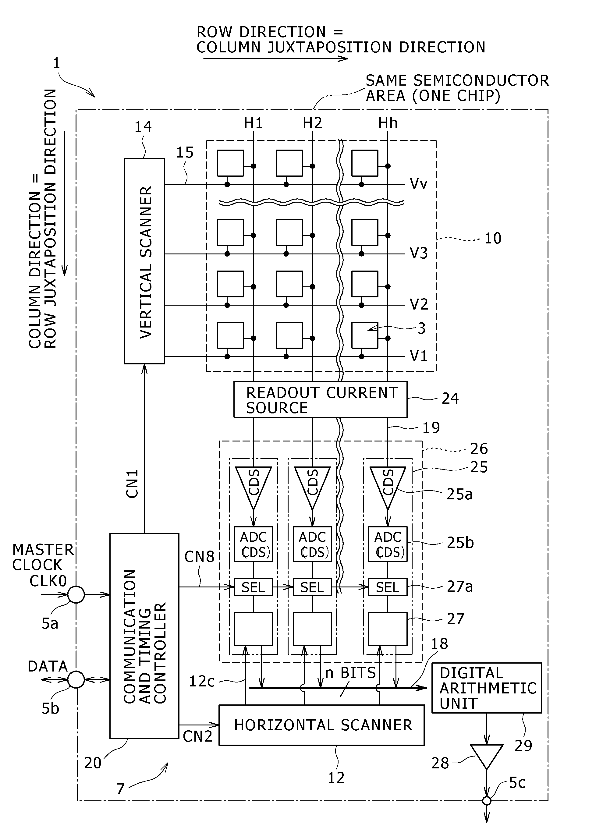
[0037]An embodiment of the present invention will be described in detail below with reference to the drawings. The following description will deal with an example in which a CMOS solid-state imaging device, which is one example of an X-Y address type solid-state imaging device, is used as the device relating to the embodiment. The description is based on an assumption that all of the pixels in the CMOS solid-state imaging device are formed of NMOS.

[0038]However, this assumption is merely one example and the device relating to the embodiment is not limited to a MOS solid-state imaging device. All of the embodiment to be described later can be similarly applied to all of semiconductor devices for detecting the distribution of a physical quantity, formed by arranging, in a line or a matrix, plural unit components having sensitivity to an electromagnetic wave such as light or radiation input from the external.

[0039]FIG. 1 is a schematic configuration diagram of a CMOS solid-state imagin...


PUM


Abstract

A method for manufacturing a solid-state imaging device in which a charge generator that detects an electromagnetic wave and generates signal charges is formed on a semiconductor substrate and a negative-charge accumulated layer having negative fixed charges is formed above a detection plane of the charge generator, the method includes the steps of: forming an oxygen-feed film capable of feeding oxygen on the detection plane of the charge generator; forming a metal film that covers the oxygen-feed film on the detection plane of the charge generator; and performing heat treatment for the metal film in an inactive atmosphere to thereby form an oxide of the metal film between the metal film and the oxygen-feed film on the detection plane of the charge generator, the oxide being to serve as the negative-charge accumulated layer.

Description

CROSS REFERENCES TO RELATED APPLICATIONS[0001]The present invention contains subject matter related to Japanese Patent Application JP 2008-037037 filed in the Japan Patent Office on Feb. 19, 2008, the entire contents of which being incorporated herein by reference.BACKGROUND OF THE INVENTION[0002]1. Field of the Invention[0003]The present invention relates to a method for manufacturing a solid-state imaging device of a charge coupled device (CCD) type, a metal oxide semiconductor (MOS) type, or a complementary metal oxide semiconductor (CMOS) type. More specifically, the present invention relates to a method for manufacturing a solid-state imaging device employing a hole accumulation (accumulated) diode (HAD) structure as a technique for preventing dark current that possibly arises in a sensor part and the periphery thereof.[0004]2. Description of the Related Art[0005]A solid-state imaging device (referred to also as an image sensor), such as a CCD image sensor and a CMOS image sens...

Claims


Application Information

Patent Timeline
IPC IPC(8): H01L31/0216H01L27/146H01L31/10H04N5/335H04N5/361H04N5/369H04N5/374
CPCH01L27/14601H01L27/14603H01L27/14689H01L27/14685H01L27/1462H01L27/146H01L21/324
Inventor HIYAMA, SUSUMUHIRANO, TOMOYUKI
Owner SONY CORP
Why Eureka
Try Eureka