

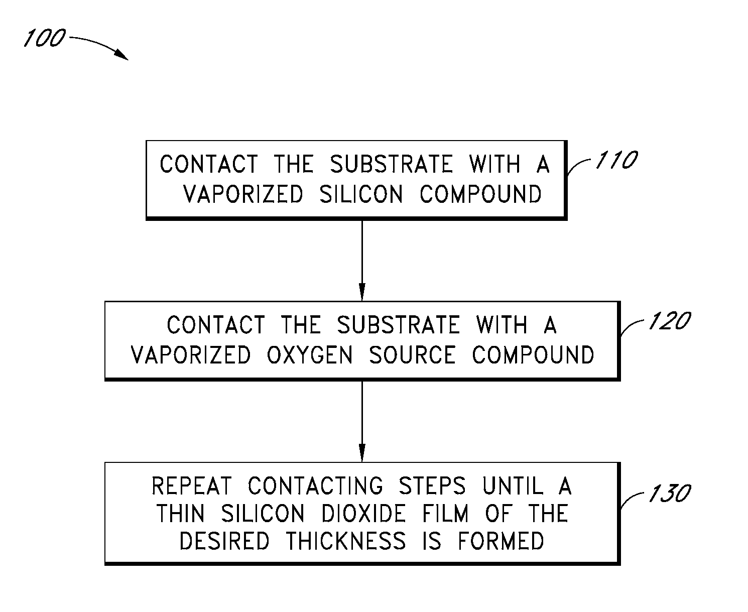
Silicon Dioxide Thin Films by ALD
a technology of silicon dioxide and thin films, applied in chemical vapor deposition coatings, coatings, metallic material coating processes, etc., can solve the problems of low rate per cycle, low conformality, and low rate per cycle of conventional cvd methods, and achieve the level of conformality and coverage desired for some applications
- Summary
- Abstract
- Description
- Claims
- Application Information
AI Technical Summary
Benefits of technology
Problems solved by technology
Method used
Image

Examples
example 1
Deposition of Silicon Dioxide from Hexakis(ethylamino)disilane and Ozone
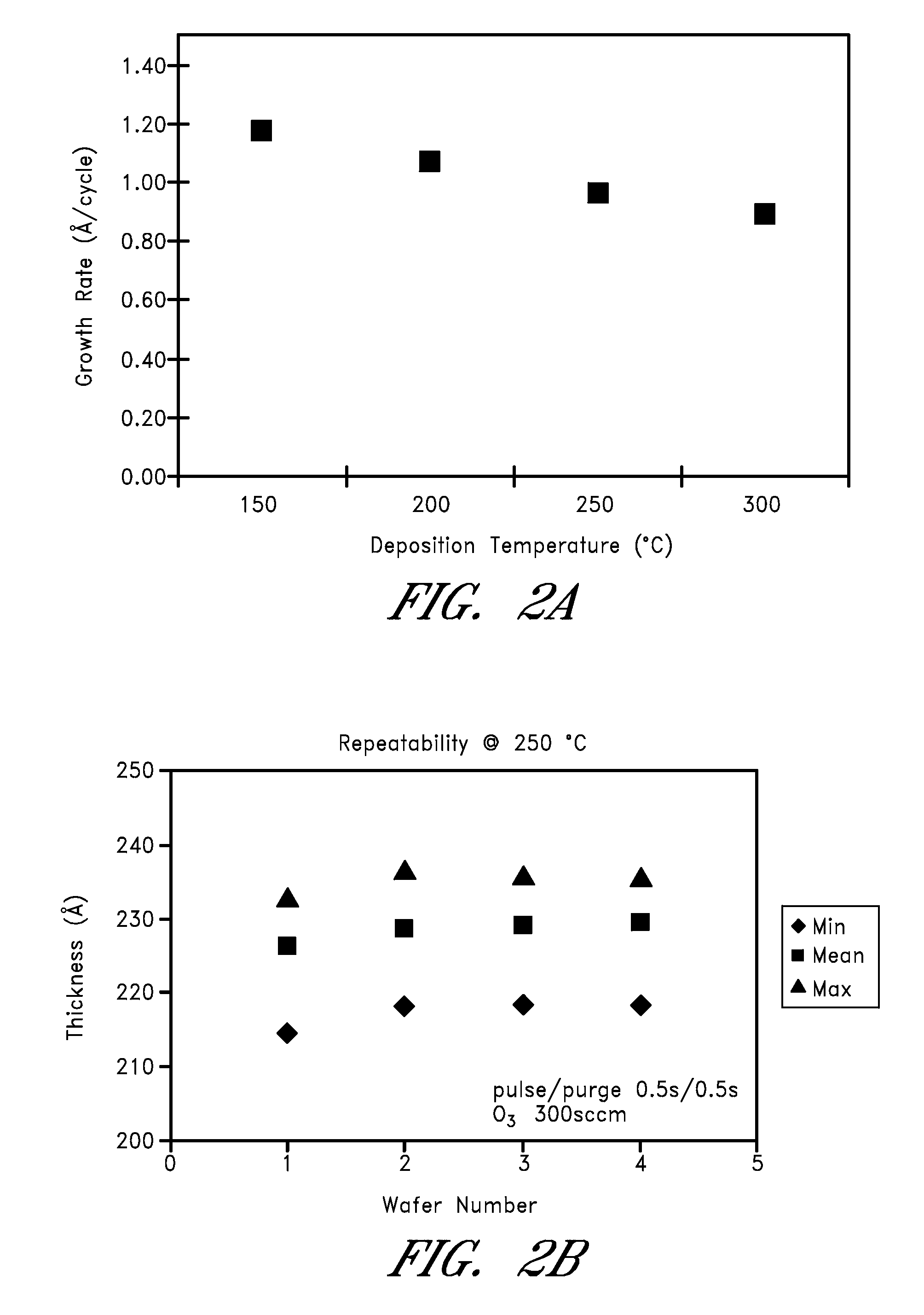
[0093]SiO2 films were deposited in an atomic layer deposition process using hexakis(ethylamino) disilane and O3. Hexakis(ethylamino) disilane is a liquid Si precursor with relatively low vapour pressure. A vaporization temperature of 110° C. was used. The deposition was carried out on 200 mm silicon wafers in an ASM Pulsar®2000 ALCVD™ reactor. Deposition temperature was varied from 150 to 300° C.
[0094]Film thickness and uniformity were measured using a spectroscopic ellipsometer. X-ray reflectometry (XRR) was also used for confirming the thickness as well as for determining the film density. The film composition was studied by both Rutherford backscattering spectroscopy (RBS) and X-ray photoelectron spectroscopy (XPS).
[0095]Growth rates (Å / cycle) at the various temperatures are presented in FIG. 2A. The repeatability of the process at 250° C. is illustrated in FIG. 2B. FIG. 3A shows the linearity of growth obser...
example 2
Deposition of Silicon Dioxide from Hexakis(ethylamino)disilane and Ozone in a Batch ALD Reactor
[0097]SiO2 films were deposited in a batch atomic layer deposition process using hexakis(ethylamino)disilane and O3. The deposition was carried out on 300 mm silicon wafers in an ASM A412™ reactor using two injectors, one for each precursor, and with a load of 120 wafers. The deposition temperature was fixed at about 300° C. The hexakis(ethylamino)disilane precursor evaporation rate was about 20 g / hr, which resulted in a flow rate of about 23 sccm from the evaporator. The evaporator was at a temperature of 148° C. The disilane precursor pulses were about 30 s. The oxygen source was ozone, with an ozone flow rate of about 3000 sccm. The ozone pulses were about 10 s. A purging and evacuation step of 10 s was used between the pulses. A scanning electron microscope (SEM) was used to determine the step coverage.
[0098]The growth rate was about 1.1 Å / cycle. Within wafer uniformities (thickness va...
PUM
| Property | Measurement | Unit |
|---|---|---|
| temperature | aaaaa | aaaaa |
| temperature | aaaaa | aaaaa |
| temperature | aaaaa | aaaaa |
Abstract
Description
Claims
Application Information