Method and Apparatus for Efficient Power Region Checking of Multi-Supply Voltage Microprocessors

Inactive Publication Date: 2009-08-20
GLOBALFOUNDRIES INC
32 Cites 9 Cited by

AI-Extracted Technical Summary

Problems solved by technology

These nested regions are more susceptible to power connection problems than other independent voltage regions.
Partial checking of just the voltage region networks is not feasible with these methods.
As a chip floor plan evolves over time to support various required design changes, power connection problems may arise for previously defin...

Method used

[0046]The software allows for a subset of its comprehensive checking capability to be used for very fast identification of flagrant voltage region interface problems. The fast algorithms steamline the checking by evaluating only a simplified or reduced number of metallurgy levels or a specific voltage domain, instead of evaluating the complete physical power structure.
[0062]To detect shorts due to a circuit abstract having metal conflicts with a voltage region's power grid, program capabilities are provided to find power metals residing over voltage regions and shorting to either (1) a circuit abstract's pin of a different net connectivity, or (2) to a circuit abstract's metal blockage. These programs speed up the checking by first finding the relevant region power metals in the full-chip power grid, and then evaluating only those metals found overlapping with a pin shape or a metal blockage shape of the same metal level that exists in the floor plan hierarchy.
[0069]The referenced annotated region properties usually represent power routing specifications. Usage of these properties can be further expanded by attaching more descriptive values to improve selective checking capabilities and performances.
[0072]The scope of this discussion is limited to validating only the physical implementation of voltage region power grid designs. However, other electrical power checking guidelines (e.g., electromigration or voltage-drop limits) can also be added as power integrity checking criteria. These guidelines can be coded on region shapes and be applicable to all circuits placed within, or they can be coded...

Benefits of technology

[0024]Therefore, the main objective of this invention is to provide an improved chip floor plan design process, with the emphasis on improving the quality of the voltage region definitions and their power distributions.
[0025]Another objective of the invention is to enable early checking results and to speed up checking for some supply problems in mu...

Abstract

A improved method for very-early validation of voltage region physical power distribution networks uses initial floor plan and early power grid data to identify physical power connection problems associated with voltage regions defined in multi-supply voltage microprocessor chip designs. Since all checking algorithms are floor plan-based and do not require complete circuit data, they are executable very early in the design phase. As a result, power region-related problems can be resolved much sooner than by using conventional full-chip physical design checking and power grid analysis methods.

Application Domain

Systems intergating technologiesComputer aided design +4

Technology Topic

Microprocessor chipPower grid +8

Image

  • Method and Apparatus for Efficient Power Region Checking of Multi-Supply Voltage Microprocessors
  • Method and Apparatus for Efficient Power Region Checking of Multi-Supply Voltage Microprocessors
  • Method and Apparatus for Efficient Power Region Checking of Multi-Supply Voltage Microprocessors

Examples

  • Experimental program(1)

Example

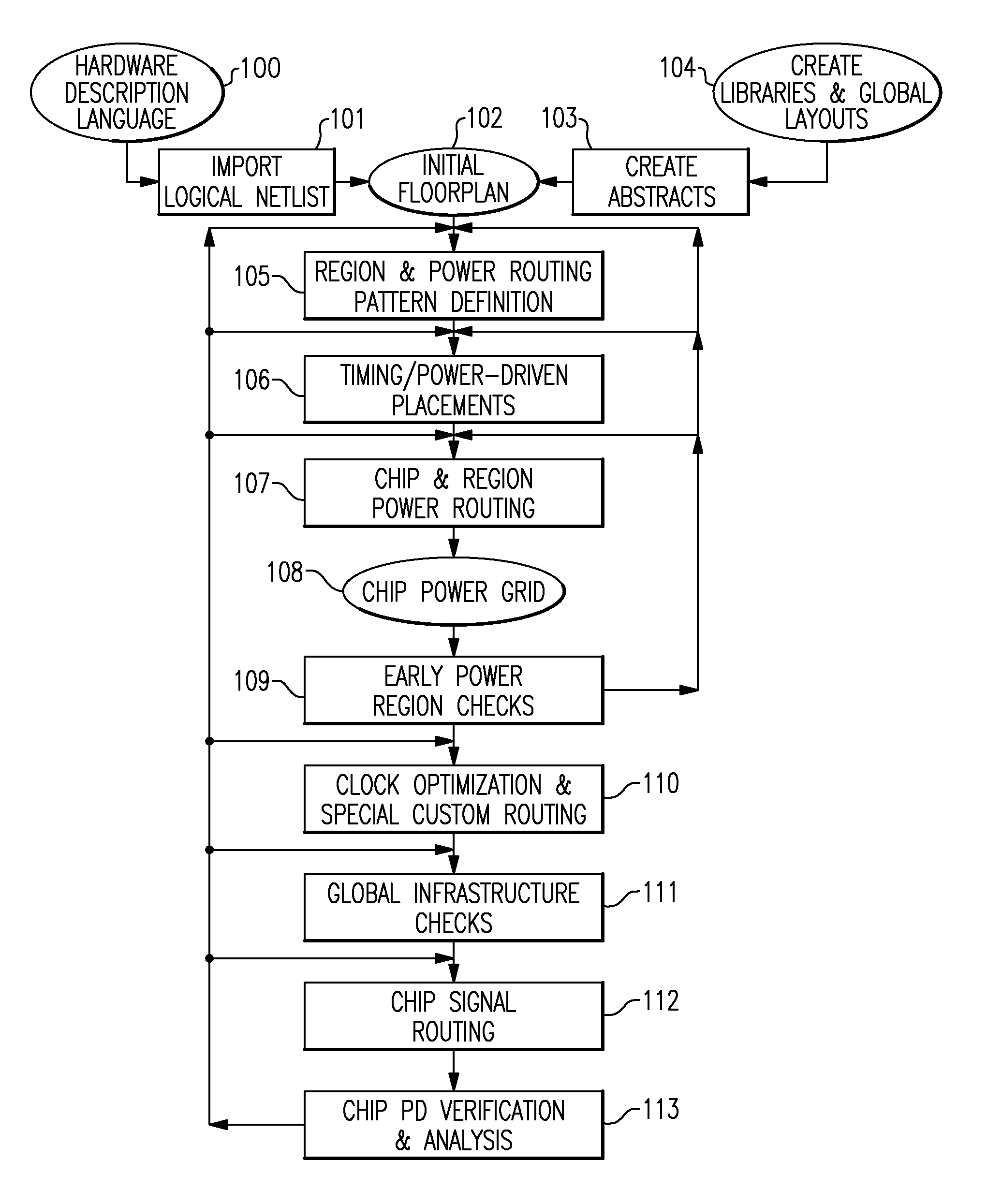
[0035]Turning now to FIG. 1, before a chip power grid 108 is created, an initial chip floor plan 102 is laid out. Custom abstract macros are created 103 and placed in the chip floorplan 102 using circuit libraries and existing global layouts 104. The floor plan 102 also contains abstract connectivity for the circuits of the floor plan imported 101 from a logical chip description 100. Floor plan power regions are defined 105, and timing-driven placements are implemented 106 to provide a skeleton from which the full-chip power routing process 107 can be used to create the chip power grid layout 108. In accordance with the present invention, after the power routing step, early power region checks 109 are performed. These tests use the early chip floor plan and power grid to detect physical power connection errors associated with voltage region designs. The tasks remaining after the early power region checks include: clock tree synthesis, optimization, and special custom routing 110; global infrastructure checks 111; and routing of chip signals 112. The global infrastructure tests 111 are performed to detect obvious conflicts between implemented chip global components. Routing of all other chip signals 112 is done after all the global infrastructure components, or their contract representations, are in place.
[0036]With a routed chip layout finally available, full-chip formal and physical design verifications 113 are performed before the design cycle is declared complete. Full-chip physical design verifications typically include LVS, DRC, and missing-power-via methodology checks (NMC), plus full-chip power grid analysis (PGA) and global signal noise analysis (GSNA). Chip power grid design errors are typically not detected until these final full-chip physical design checks are performed. By introducing the EPRC toolset 109 into the typical chip design flow as shown in FIG. 1, voltage region power grid design errors can be detected much earlier for correction. Usage of this invention is especially beneficial to the early chip floor planning process, in particular, the optimization of voltage region definitions. Continuous evaluations of early voltage region power distribution networks help to fine-tune the region boundaries, their circuit compositions as well as their power routing patterns.
[0037]As shown in FIG. 1, errors detected by the early power region checks 109 and the chip physical design and analysis 113 are fed back to previous stages for correction. As a result, errors detected by the chip physical design variation and analysis will be checked by the early power region checks.
[0038]Turning now to FIG. 2, this flowchart illustrates a quick checking method, which detects a power region short that usually occurs due to conflicting definitions of region areas and/or power routing patterns. Based on properties already coded on region shapes 200, the program determines the regions' highest levels of metal 201. From the full-chip power grid 202, the program identifies locations of defined voltage regions 203. For each voltage region, the program allocates metals of the identified region's highest level 204. For each identified metal of the region-under-test, find other overlapping metals of the same level 205. If any such overlapping metal exists, check power connectivity of the overlapping metal 206. If connectivity of the overlapping metal is different from the region's metal-under-test, the program flags the region's metal shape as a short and the region shape as a region having power shorts 207. The check repeats for all metals found in this region on its expected highest level of routing layer 208.
[0039]FIG. 3 illustrates a preferred quick power region continuity check, which detects a common type of uncovered (i.e., unconnected or open) power region due to missing power connections between the region's power grid and its parent power distribution network. Similar to FIG. 2, region shapes and properties 300 are used to determine the region's highest metal level and their associated power domains 301. From the full-chip power grid 302, region metals of the identified highest level are found 303. If none is found 304, the region is flagged as an open 307 (as this type of problem is likely due to outdated power distribution network versus its defined routing specification). If highest region metals are found, unique metal connectivity information is extracted from the allocated metals 305, and compared 306 against the list of power domains already derived from region properties for each expected region metal level 301. If a mismatch is found, the region shape is flagged as having power open 307.
[0040]FIG. 4 illustrates a preferred quick power region continuity check, which detects a flagrant type of uncovered power region due to a missing power supply in the implemented physical region power distribution networks. This type of error is usually due to obsolete power grid data or to conflicting region specifications. Similar to previous examples, region shapes and properties 400 are used to determine metal levels expected for each region and power domains for each of these levels 401. From the full-chip power grid 402, for each identified region's metal level, the program allocates metals of that level 403. If none is found 404, the region is flagged as an error 407 on that metal level against its routing specifications. If region metals are found, their metal connectivity is checked 405. For each expected power domain of that metal level, at least one metal must exist with its connectivity matching the expected region domain 406. If no metal is found with connectivity matching an expected region domain, the region shape is identified as having power open 407.
[0041]FIG. 5 and FIG. 6 illustrate power short checks, which detect a region power metal shorting, respectively, to a macro's metal blockage and to a macro's pin inside voltage regions. In both flowcharts, region shapes 500 and 600 are used to determine the locations of the corresponding voltage region power distribution networks 503 and 603 in the full-chip power grid 502 and 602. For each requested checking metal level, using the chip floor plan, which contains circuit abstract placements and connectivity as an input 501 and 601, the program finds metals overlapping, respectively, either with a circuit's blockage shape of the same metal 504, or with a circuit's pin shape of the same metal 604. As depicted in FIG. 5, if a region metal overlapping a circuit's macro blockage is found 505, both the region shape and region metal are flagged as having an error and power short 506 and 507. For power shorting with circuit's pins, FIG. 6 shows that macro pin connectivity 606 also has to be obtained from the floor plan and checked against the region's metal connectivity 607. If connectivity mismatches exist, the circuit macro whose pins are shorting with the region's metal is flagged as an error 608. Similarly, the macro's region shape is also flagged as having and error and macro power shorts within 609 and 610. Both processes end 509 and 612 when there is no more metal to check 508 and 611.
[0042]FIG. 7 illustrates a power region continuity check, which identifies uncovered macro power distribution networks by comparing circuit power domains against the region power domains using data in the chip floor plan 700 and chip power grid layout 704. For all circuits that are placed inside a voltage region 701, circuit power domains can be derived from actual macro pin connectivity 703 and 705 already existing in the floor plan 700. For all voltage regions being checked, region power domains are determined as depicted in FIG. 7 based on region metal connectivity 706. Alternately, this information can also be quickly determined based on properties coded on corresponding region shape 703. If a mismatch 708 is found between a macro's power domain 702 and the region's power domains 706, both the macro abstracts and the corresponding region shape are flagged as errors 709. The process ends 711 when there are no more domains to check 710.
[0043]FIG. 8 illustrates a power region continuity check, which identifies uncovered macro power distribution networks by checking a circuit abstract's highest level of power metals for minimum connection with its parent power distribution network. Here, after the circuit power domain and the circuit's highest power level of metal are determined from the chips floor plan 100 in steps 801, 802 and 803, region metals of the next higher level are allocated by the checking program 806 and 807. For all region metals of the next higher level that are found overlapping the macro, the macro is considered a potential problem 808 if none has matching connectivity as the macro power pins. Its identified power pins are then checked for overlapping the macro pin extensions of the same metal level and same connectivity, and that these extensions have connections to the next higher level of metal in the vicinity of the macro and/or the region's boundary 809. If the last two criteria fail, both the macro and the corresponding region shapes are identified as errors 810, 811. The check repeats for each power domain found on highest metal of the circuit abstract 812.
[0044]Using existing connectivity data in the chip power grid and based on the technology metallurgy characteristics, the invention's checking algorithms can detect most types of real voltage region power shorts and opens without having to build a full logical representation of the complete full chip power metallurgy and power via structure as typically required by conventional full chip LVS and PGA checking processes.
[0045]For quick validation of macro related power connections inside voltage regions, the invention makes use of logical power net connectivity data already existing in the input chip floor plan. Macro power net connectivity data are automatically coded by a computer aided process that translates and imports the full chip logical description, usually coded in a hardware description language, into the graphical chip floor plan in the physical design database.
[0046]The software allows for a subset of its comprehensive checking capability to be used for very fast identification of flagrant voltage region interface problems. The fast algorithms steamline the checking by evaluating only a simplified or reduced number of metallurgy levels or a specific voltage domain, instead of evaluating the complete physical power structure.
[0047]The above described a set of physical design checking programs are applicable to checking a stand-alone chip power grid or to a chip power grid against an input chip floor plan.
[0048]This set of checking programs can analyze a routed chip power grid and identify real power shorts and opens that exist in voltage regions. These checks uncover problems that are typically due to an inconsistent interface defined between region and chip power distribution networks or between overlapping or nested voltage regions.
[0049]Others of the checking programs in the set are also available to validate region compositions in a chip floor plan. Here, voltage region power distribution networks in a routed chip power grid are checked against an input chip floor plan. These checks detect insufficient or incorrect interactions between the power image of the circuits placed inside voltage regions and the physical power distribution networks residing over the corresponding voltage regions. The checks validate the physical connections of the power distribution networks to the macro pins against the logical connectivity information that exist in the chip floor plan for all macro pins. These checks uncover problems that are typically due to floor planning or circuit abstract changes.
[0050]Both of the above types of checks use region shapes to identify the locations and areas of the associated physical power grid distribution networks in a full-chip power grid. Region shapes are non-manufacturing shapes used to represent voltage regions of independent power domains. These shapes are usually drawn directly in the input chip floor plan to encompass the intended region compositions. They can also be created in the chip power grid layout, or in an independent region specification cell view, whose area and coordinates are equivalent to that of the chip floor plan. All region shapes must be coded with power metallurgy routing properties to distinguish themselves as region shapes
[0051]Using region power routing properties, which include the expected region power domains and the region metallurgy characteristics, as checking specifications, the invention provides quick checking algorithms to detect errors for applicable region metal layers against their expected interfaces.
[0052]As pointed out previously, the power connection checking algorithms use power net connectivity data that already exist in the chip power grid. Applicable region power metal levels are checked in succession against the metals above and/or below based on technology metallurgy characteristics.
[0053]All of the above checking algorithms can be limited to a certain power region of interest, a region metal layer, and/or a region domain type.
[0054]The program capabilities listed below are available for checking voltage region power distribution networks. These programs are intended to be executed against a stand-alone input chip power grid layout.
[0055]To detect shorts that exist in region power distribution networks, program capabilities are provided to find power stripes of the same metal level but of different power domains connecting with each other within a voltage region boundary. In general, these programs (1) find the relevant region power metals based on region shapes and their coded properties; (2) find overlapping of the identified region metals with other power metals in the chip power grid of the same level and the same connectivity; and (3) highlight all region metals that have overlapping metals of same metal but different connectivity as shorts.
[0056]A frequently used default programming checking mode for the above is to find shorts for all routing metals defined for the voltage region. Although the advanced algorithmic power routing technique typically guarantees no short for the routing metal hierarchy, execution errors may still result in conflicts between newly routed voltage region distribution networks versus an existing full-chip power grid.
[0057]A default quick programming checking mode for the above is to find shorts for the region's highest metals. This is because most common region power shorts are due to the interface between the region's highest metal and the next metal of its parent distribution network or of a nested or overlapping voltage region.
[0058]To detect opens that exist in region power distribution networks, program capabilities are provided to find region power stripes that have no connection to the expected next level of metal. The checking algorithms take into account that power domains may vary for each metal level. For instance, a complex multi-supply voltage region may have a higher level of metal supporting multiple voltage supplies while a lower level needs to support just one specific power domain. This is because connections to the higher metal for the lower level may be accomplished outside the region and still adequately address the power demand of connected circuits. In general, these programs (1) find relevant region power metals based on region properties; (2) identify those region metals that overlap with other metals of same connectivity but of the next level of metal; and (3) highlight all region power metals that do not have any such overlap as power opens.
[0059]A default quick programming checking mode above is to find all of the region's highest metals that do not overlap (i.e., connect) with any metal of the next higher level of the same connectivity. This is because the region's highest routing metal is typically required to have a direct interface with its parent physical power distribution network. The same power continuity check can be performed for a region's metal versus both the next higher and lower levels of metal. However, unless the region's metal-under-test is already the technology's top level of metal, for an advanced chip design with robust power routing technology, checking the region's highest power metal versus the next lower metal is usually not necessary.
[0060]Another default quick programming checking mode above is to identify an obviously missing power domain in the region's physical power grid. Using coded region properties, the checking program determines the expected domains for each region routing metal level. The program then quickly verifies for existence of all expected metal levels in the physical power distribution networks and their expected power domains based on the metal connectivity information. If an expected domain is missing from a routed metal level, the region is flagged as having power opens.
[0061]The program capabilities listed below are available for checking voltage region power connections versus region circuit compositions. These programs are intended for analyzing voltage region distribution networks that already exist in an input chip power grid layout against the region compositions found in an input chip floor plan. The chip floor plan contains circuit macro abstracts and power pin connectivity of all abstracts.
[0062]To detect shorts due to a circuit abstract having metal conflicts with a voltage region's power grid, program capabilities are provided to find power metals residing over voltage regions and shorting to either (1) a circuit abstract's pin of a different net connectivity, or (2) to a circuit abstract's metal blockage. These programs speed up the checking by first finding the relevant region power metals in the full-chip power grid, and then evaluating only those metals found overlapping with a pin shape or a metal blockage shape of the same metal level that exists in the floor plan hierarchy.
[0063]For shorting to a circuit abstract's pins, after finding the overlapping region's power metals with an abstract's pin shape, the checking algorithm (1) extracts the abstract pin's connectivity attribute in the chip floor plan; (2) compares the extracted attribute with that of the overlapping region's power metal; and (3) flags the region's power metal as a short if the compared connectivity attributes are not the same.
[0064]For shorting to a circuit abstract's blockage, the checking algorithm flags the region's power metals that overlap with the blockage shape as a short. This is because metal blockage shapes represent metal resources reserved for signal routing.
[0065]To detect the macro's power opens in voltage regions, quick checking program capabilities are provided to ensure minimum power connection between the macro's power pins and the region's power grid. The checking algorithms take into account that there are two methods of connecting a macro's power pins to its parent power grid: (1) Macro pins directly connecting to the next level of metal of same connectivity overlapping with the pins, and/or (2) Macro pins indirectly connecting to the next level of metal of same connectivity existing outside the macro boundary. The latter method makes the connection by first creating “macro pin extensions,” which are power wires of the same metal level as the macro pins, and connecting the macro pins to the nearest region's next level of metal having the same power connectivity. In general, these checking programs: (1) find circuit abstracts residing in voltage regions; (2) find relevant power pins of each circuit abstract; (3) for each circuit's power domain, find next-higher metals of same power connectivity residing over this circuit boundary in the region; (4) if none found, check for macro power pin extension of same power connectivity and power metal level as the circuit's highest metal power pin; and (5) if none found, the circuit is flagged as having insufficient power connection.
[0066]The default quick programming checking mode for the above is to check only the highest metal power pins of the circuit abstracts. This is because the circuit's highest level of metal is typically required to have a direct interface with its parent distribution network, while the internal physical macro power grid is usually required to be error-free by the circuit's design methodology.
[0067]Another default quick programming checking mode for the above is to identify obviously invalid macro power domain types. Using coded region properties, the checking program determines the expected domains for each region. Using the chip floor plan, the program extracts power domains for all circuit macros placed within a voltage region. If a macro's power domain is not part of the region domains, the macro and the region are flagged as having power open.
[0068]The tools and algorithms implemented for this invention make use of region shapes and their annotated power routing properties coded in a graphical input cellview (e.g., the chip floor plan, the chip power grid, or an independent region specification cell view). However, the same information may also be obtained from a separate input file. Alternate programming data structures can also be defined to represent these region properties in the graphical physical design database.
[0069]The referenced annotated region properties usually represent power routing specifications. Usage of these properties can be further expanded by attaching more descriptive values to improve selective checking capabilities and performances.
[0070]Technology metallurgy structure, such as upper and/or lower metals associated with each metal-under-test, is updateable for use by all existing checking algorithms. This capability is to support reuse of program capabilities in any new metal technology.
[0071]The described checking toolset is constructed to allow additions of other voltage-island integrity checks such as (1) desired ratio for routing multi-domain power regions (e.g., 3 VIO to every 1 VDD wiring track on a certain high metal layer, but only VDD for all lower metals) depending on the region composition; (2) maximum recommended distance of a custom macro to be placed inside a voltage region to the nearest corresponding power IO-pad; (3) desired ratio of certain power IO-pads within a region boundary; or (4) maximum allowed vicinity of power connections for a macro placed within a region to the next level of metal outside a voltage region.
[0072]The scope of this discussion is limited to validating only the physical implementation of voltage region power grid designs. However, other electrical power checking guidelines (e.g., electromigration or voltage-drop limits) can also be added as power integrity checking criteria. These guidelines can be coded on region shapes and be applicable to all circuits placed within, or they can be coded for specific circuits placed inside regions. For example, a circuit macro's power or current estimate can be coded for the macro and be checked against a recommended distance to nearest relevant power IO-pad, or to the nearest power of a certain high-metal (e.g., metal-9, which directly connects to the IO-pad's metal-10) to ensure good power distribution from the corresponding IO-pad to the circuit-under-test.
[0073]The cost and time savings in the overall design cycle were accomplished by (1) enabling checking of voltage region distribution networks independently, and by (2) using early chip floor plan and power grid connectivity data. Since voltage region design problems are identified much earlier using this invention, power regions and/or their macro placements can be fine-tuned or corrected much sooner than possible with the conventional full-chip physical design checks. Full-chip physical design checks require more complete circuit design data. These are typically very time- and memory-consuming processes. They also require extra analysis to isolate voltage region design problems from reported errors. Also, in design environments where full chip checking capability of multi-voltage chip designs are still limited, the invention helps preventing flagrant voltage region power connection problems from being deployed in actual hardware.
[0074]Because macro abstract information is used instead of actual circuit layouts, and power grid connectivity and metallurgy characteristics are used instead of building the complete chip power metallurgy and power via structure, the invention flags power grid and macro-related power shorts and opens that exist in voltage regions much faster and more comprehensively than existing LVS-continuity (LVSC) based checks.
[0075]For power shorts, the invention is able to identify all problems for any metal level associated with a voltage region. Alternately, the invention also identifies all at once all the circuits in a voltage region that have either power domain or metal conflicts with the region or the chip power grid. This checking capability is a major time-saving for detecting power shorts versus conventional LVSC-based checks, which detect only one short at a time and require additional analysis to isolate the actual source of problems.
[0076]The invention is applicable to a specific power region, a region metal layer, and/or a region domain type. Checking algorithms are readily re-usable for a chip design with a newer metal technology. This is achievable by simply updating the metallurgy structure characteristics (i.e., the upper and lower metals associated with a metal-under-test) corresponding to the newer technology.
[0077]In controlled EC design mode, the invention identifies any new voltage region power grid problem that may surface due to a placement or abstract change. This helps to determine the magnitude of the change required to correct the problems with minimum effort.
[0078]The present invention is implemented by a computer. It contains software that validates physical voltage region power distribution networks to be built in hardware as part of a full chip power grid layout. The software can be contained on media usable by the computer such as tangible, optical and magnetic media.
[0079]There may be many variations to the diagrams and the steps (or operations) described herein without departing from the spirit of the invention. For instance, the steps may be performed in a different order, or steps may be added, deleted or modified. All of these variations are considered a part of the claimed invention. Therefore while the preferred embodiment to the invention has been described, it will be understood that those skilled in the art, both now and in the future, may make various improvements and enhancements that fall within the scope of the claims that follow.

PUM

no PUM

Description & Claims & Application Information

We can also present the details of the Description, Claims and Application information to help users get a comprehensive understanding of the technical details of the patent, such as background art, summary of invention, brief description of drawings, description of embodiments, and other original content. On the other hand, users can also determine the specific scope of protection of the technology through the list of claims; as well as understand the changes in the life cycle of the technology with the presentation of the patent timeline. Login to view more.

Similar technology patents

Techniques for automated database deployment

ActiveUS9946534B1quickly identify
Owner:JPMORGAN CHASE BANK NA

Tissue processing apparatus with mixing device and method for processing adipose tissue

ActiveUS20150352256A1quickly identifyquickly determine
Owner:THE GID GROUP

Laser marker

InactiveUS20140340725A1quickly identify
Owner:TANG ZHEN

Endodontic rotary instruments for preparing root canal spaces

InactiveUS20080176191A1easily choosequickly identify
Owner:ENDODONTIC EDUCATIONAL SEMINARS

Physical cable lead identifier for medical systems

ActiveUS9522048B1high noise levelquickly identify
Owner:GENERAL ELECTRIC CO
Why Eureka
Try Eureka