

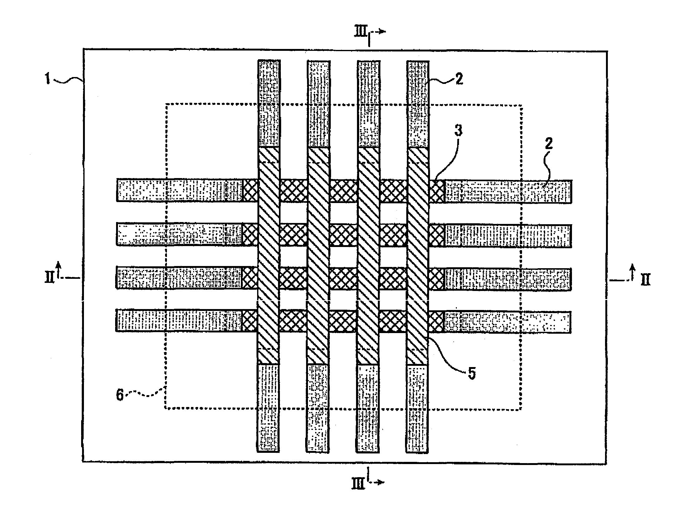
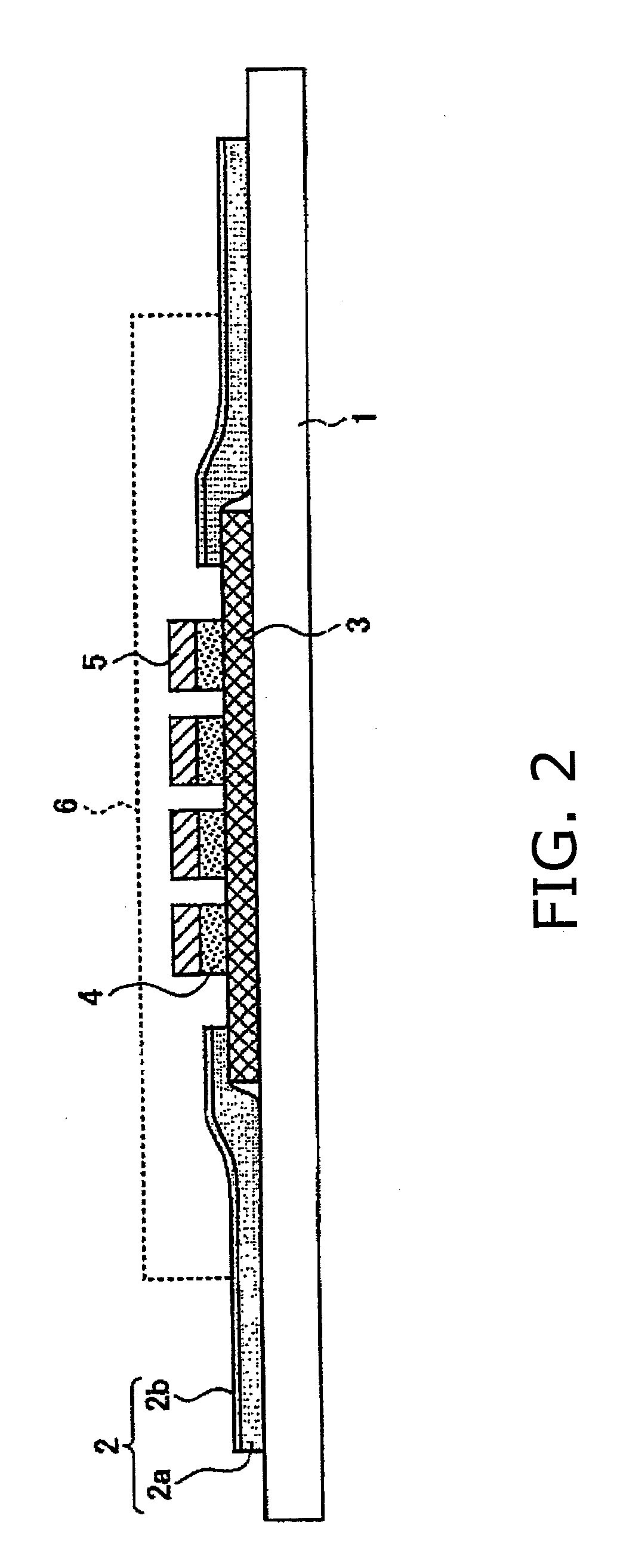
Laminate for forming a substrate with wires, substrate with wires and methods for producing them
a technology of a substrate and a wire, which is applied in the direction of identification means, instruments, transportation and packaging, etc., can solve the problems of easy electrochemical reaction to ito, difficult to reduce the specific resistance below about 4cm, and the resistance of the ito layer is now approaching the limit, so as to prevent the deterioration of reduce the voltage necessary to drive the flat panel display, and reduce the contact resistance between the conductive protection layer and the catho
- Summary
- Abstract
- Description
- Claims
- Application Information
AI Technical Summary
Benefits of technology
Problems solved by technology
Method used
Image

Examples
example 1
[0080]Soda lime glass substrates having a thickness of 0.7 mm were cleaned and they were fixed on a sputtering device. A high frequency magnetron sputtering method was carried out by using a silica target to form a silica layer having a thickness of 20 nm on the substrates. Thus, substrates with a silica layer were obtained.
[0081]Then, on each of the substrates with a silica layer, an ITO layer having a thickness of about 160 nm was formed according to a d.c. magnetron sputtering method by using an ITO target (containing 10 mass % of SnO2 based on the total amount of In2O3 and SnO2). Thus, substrates with an ITO layer were obtained. The composition of the ITO layer was substantially the same as that of the ITO target.
[0082]Further, on each of the substrates with an ITO layer, a 99Ag-1Pd (atomic %) alloy layer having a thickness of about 300 nm was formed as a conductor layer in an atmosphere of Ar gas according to a d.c. magnetron sputtering method by using a silver / palladium alloy ...
examples 2 to 5
[0083]On each of the substrates with a conductor layer obtained in Example 1, an IZO layer as shown in Table 1 was formed as a conductive protection layer by d.c. magnetron sputtering method in an atmosphere of Ar gas by using an IZO target (containing 10.7 mass % of ZnO based on the total amount of In2O3 and ZnO). Thus, laminates for forming substrates with wires were obtained. The conditions of sputtering were 0.6 Pa for sputtering pressure, and 200° C. for film-forming temperature (substrate temperature). The composition of the IZO layer was substantially the same as that of the IZO target.
1-2. Evaluation of UV / O3 Resistance of Laminates for Forming Substrates with Wires, etc.
[0084]To the substrates with a conductor layer obtained in Example 1 and laminates for forming substrates with wires obtained in Examples 2 to 5, patterning is conducted according to a photolithographic method to form wires having a width of 50 μm. Thus, substrates with wires were obtained. Each etching time...
examples 6 to 8
[0088]On each of the substrates with a silica layer obtained in Example 1, a 99Ag-1Pd (atomic %) alloy layer having a thickness of about 380 nm was formed as a conductor layer in an atmosphere of Ar gas according to a d.c. magnetron sputtering method by using a silver / palladium alloy target (99Ag-1Pd (atomic %)) to thereby obtain substrates with a conductor layer. The conditions of sputtering were 5×10⁻⁴ Pa for back pressure, 0.5 Pa for sputtering pressure and 200° C. for film-forming temperature (substrate temperature).
[0089]On each of the substrates with a conductor layer, an IZO layer having a thickness of about 30 nm was formed as a conductive protection layer according to a d.c. magnetron sputtering method by using an IZO target (containing 10.7 mass % of ZnO based on the total amount of In2O3 and ZnO) to obtain laminates for forming substrates with wires. The conditions of sputtering were 0.6 Pa for sputtering pressure and 200° C. for film-forming temperature (substrate temper...
PUM
| Property | Measurement | Unit |
|---|---|---|
| thickness | aaaaa | aaaaa |
| thickness | aaaaa | aaaaa |
| thickness | aaaaa | aaaaa |
Abstract
Description
Claims
Application Information