

Advanced process sensing and control using near infrared spectral reflectometry
a technology of near infrared spectral reflectometry and process sensing, applied in the direction of optical radiation measurement, interferometric spectrometry, instruments, etc., can solve the problem of inability to meet the needs of next-generation process conventional measurement processes
- Summary
- Abstract
- Description
- Claims
- Application Information
AI Technical Summary
Benefits of technology
Problems solved by technology
Method used
Image

Examples
Embodiment Construction
[0032]While embodiments described herein are exemplarily described as an etch process performed in an etch chamber, it is contemplated that aspects described herein may be used in other chambers and processes. Examples include deposition chambers, such as epitaxial deposition chambers, chemical vapor deposition (CVD) chambers, plasma enhanced chemical vapor deposition (PECVD) chambers, physical vapor deposition (PVD) chambers, and the like. Other processes include plasma treating and rapid thermal processing (RTP) chambers, among other processes utilizing high temperatures and / or a need for real-time monitoring of process parameters.
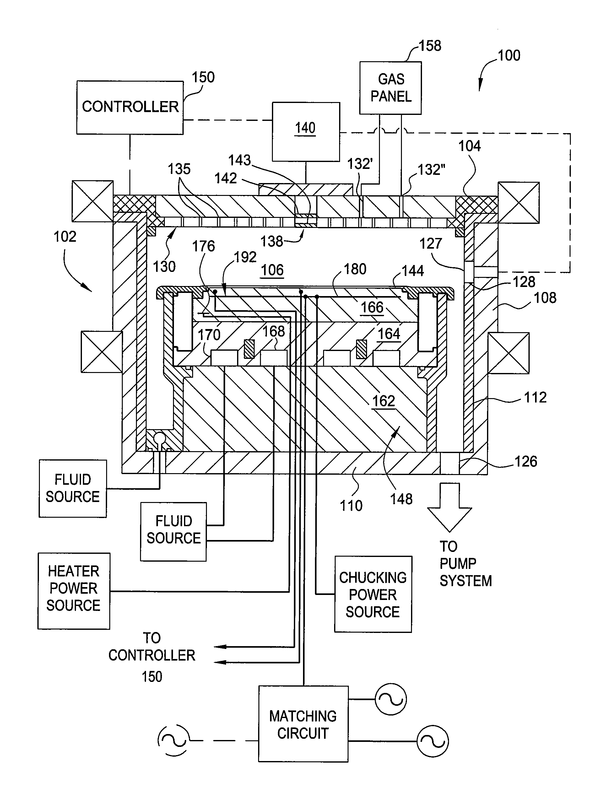
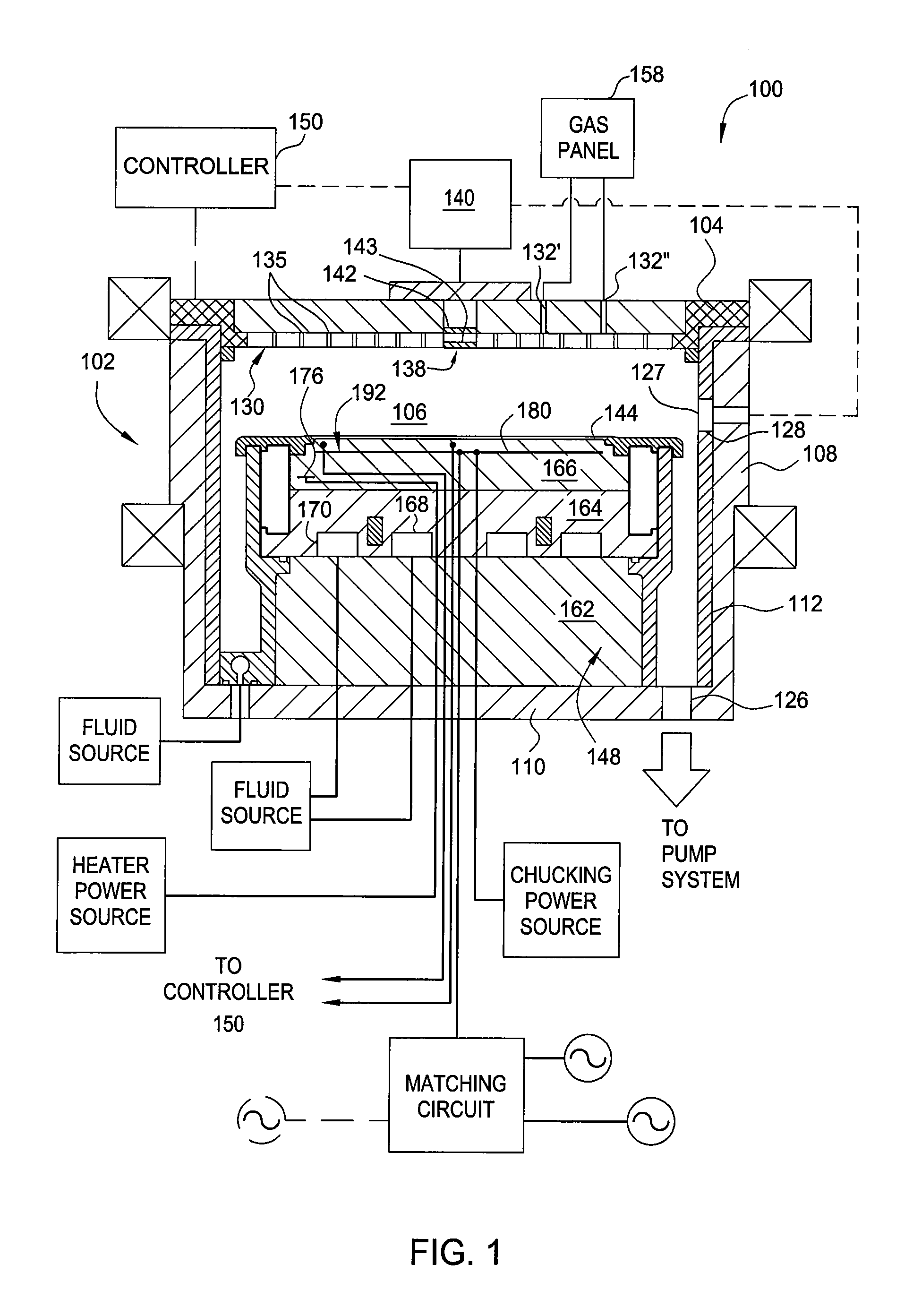
[0033]FIG. 1 is a sectional view of one embodiment of an exemplary processing chamber 100 adapted as a plasma chamber. In one embodiment, processing chamber 100 is suitable for etching high aspect ratio features in a substrate 144. The processing chamber 100 includes a chamber body 102 and a lid 104 which bounds a processing volume 106. The chamber body ...
PUM
| Property | Measurement | Unit |
|---|---|---|
| Angle | aaaaa | aaaaa |
| Volume | aaaaa | aaaaa |
| Energy | aaaaa | aaaaa |
Abstract
Description
Claims
Application Information