Semiconductor device and electric apparatus

a technology of semiconductor devices and diodes, which is applied in semiconductor devices, diodes, power conversion systems, etc., can solve the problems of reverse recovery time delay and reverse recovery time delay of parasitic diodes operation, and achieve high-speed switching operation and energy loss reduction, and excels in resistance to current concentration

Active Publication Date: 2009-09-10
PANASONIC CORP
View PDF11 Cites 35 Cited by
  • Summary
  • Abstract
  • Description
  • Claims
  • Application Information

AI Technical Summary

Benefits of technology

[0035]The present invention can provide a semiconductor device and an electric apparatus each of which can realize both high-speed switching operation and energy loss redu

Problems solved by technology

However, even in the case of the SiC-MISFET, by a parasitic diode comprised of a PN junction of a P-type region and an n-type region in a semiconductor device, a reverse recovery time delay may occur in the case of switching from an ON state of the parasitic diode to an OFF state of the SiC-MISFET when a reverse bias is applied.
For example, when a

Method used


Image

  • Semiconductor device and electric apparatus
  • Semiconductor device and electric apparatus
  • Semiconductor device and electric apparatus

Examples


Embodiment Construction

[0074]Hereinafter, a preferred embodiment of the present invention will be explained with reference to the drawings.

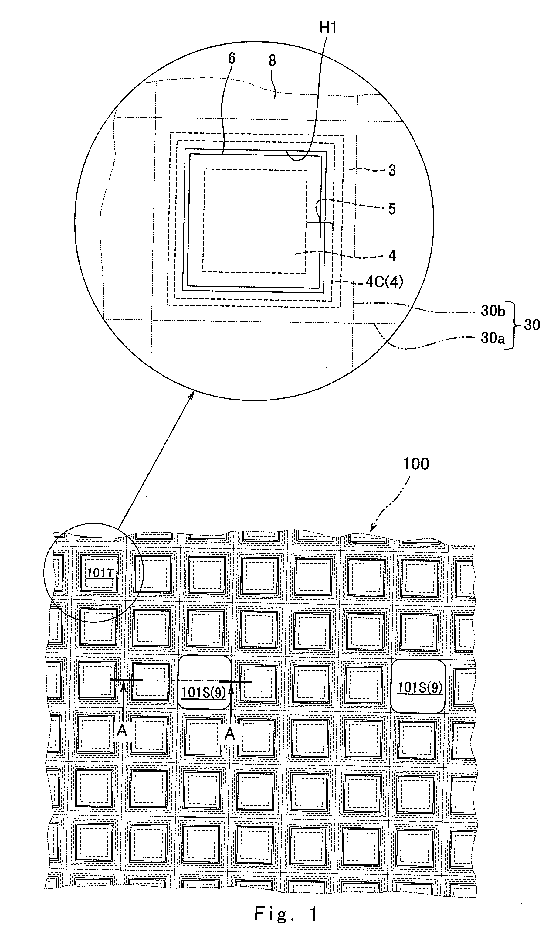
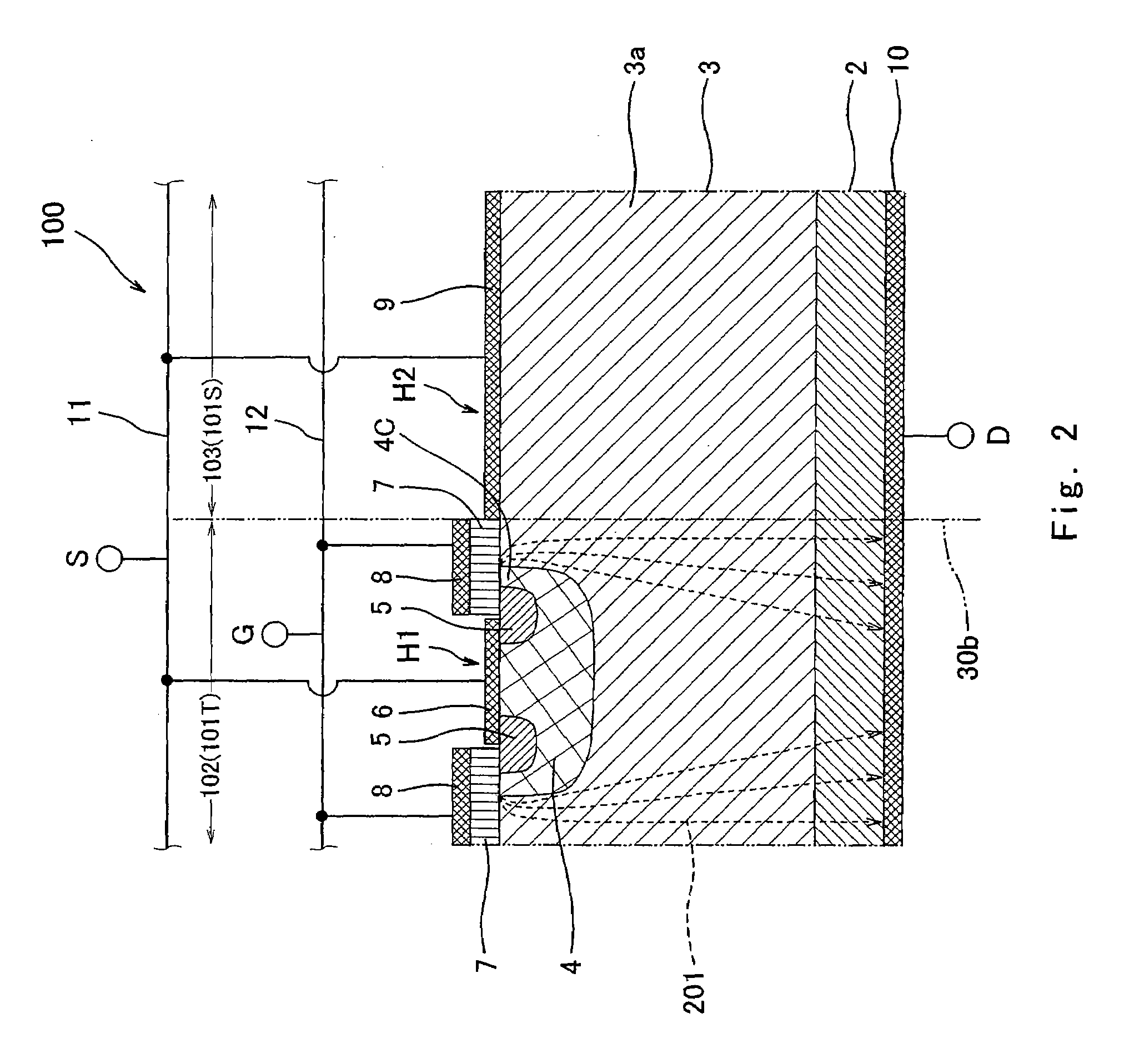
[0075]FIG. 1 is a plan view showing one example of a construction of a semiconductor device according to an embodiment of the present invention. FIG. 2 is a sectional view of the semiconductor device as taken along line A-A of FIG. 1. In the following explanation, “n” and “p” denote a conductivity type, and in such type of layer or region, electrons or positive holes are carriers. In addition, “+” denotes high impurity concentration, and “−” denotes low impurity concentration.

[0076]As shown in FIGS. 1 and 2, in a semiconductor device 100 in plan view, a SiC layer 3 (semiconductor layer) is constructed such that a plurality of quadrangular (square, herein) subregions 101T and 101S are arranged evenly (equal area) in a matrix manner in two directions intersecting (orthogonal to) each other by a plurality of border lines 30 comprised of virtual horizontal border lines 30a...


PUM


Abstract

The present invention provides a semiconductor device and an electric apparatus each of which can realize both high-speed switching operation and energy loss reduction and excels in resistance to current concentration based on a counter electromotive voltage generated by, for example, an inductance load of the electric apparatus. A semiconductor device (100) of the present invention includes: a semiconductor layer (3) made of a first conductivity type wide band-gap semiconductor; a transistor cell (101T) in which a vertical field effect transistor (102) is formed, the vertical field effect transistor (102) causing a charge carrier to move in a thickness direction of the semiconductor layer (3); and a diode cell (101S) in which a schottky diode (103) is formed, the schottky diode (103) being formed such that a schottky electrode (9) forms a schottky junction with the semiconductor layer (3), wherein the semiconductor layer 3 is divided into a plurality of square subregions (101T and 101S) based on virtual border lines (30) in plan view, and includes the subregion (101T) as the transistor cell and the subregion (101S) as the diode cell.

Description

TECHNICAL FIELD[0001]The present invention relates to a semiconductor device and an electric apparatus, and particularly to an improvement technology of a power semiconductor device used for inverter control of various electric apparatuses.BACKGROUND ART[0002]In light of an energy loss reduction, a wide band-gap semiconductor (such as silicon carbide (SiC)) are attracting attention as a semiconducting material which goes beyond the limit of an existing Si power field effect transistor (hereinafter referred to as “Si-MISFET”).[0003]Since a SiC semiconductor has a wide band gap, a drift region of a power field effect transistor (hereinafter referred to as “SiC-MISFET”) made of the SiC semiconductor has an excellent high withstand voltage performance. This realizes the reduction in thickness of the drift region which plays an important role to improve a conduction loss caused due to the decrease in an on-resistance (Ron) per unit area of a semiconductor device while securing a certain ...

Claims


Application Information

Patent Timeline
IPC IPC(8): H02M7/5387H01L29/161
CPCH01L29/0696H01L29/1602H01L29/1608H01L29/7806H01L29/47H01L29/66068H01L29/2003
Inventor KITABATAKE, MAKOTO
Owner PANASONIC CORP
Why Eureka
Try Eureka