

Scanning electron microscope
a scanning electron microscope and microscope technology, applied in the direction of instruments, material analysis using wave/particle radiation, heat measurement, etc., can solve the problems of inability to form the entire thickness to several mm or less, and the distance (working distance, wd) from the lower surface of the objective lens to the sample cannot be shorter than the thickness of the detector, so as to improve the response, save cost and space, and facilitate assembly
- Summary
- Abstract
- Description
- Claims
- Application Information
AI Technical Summary
Benefits of technology
Problems solved by technology
Method used
Image

Examples
first embodiment
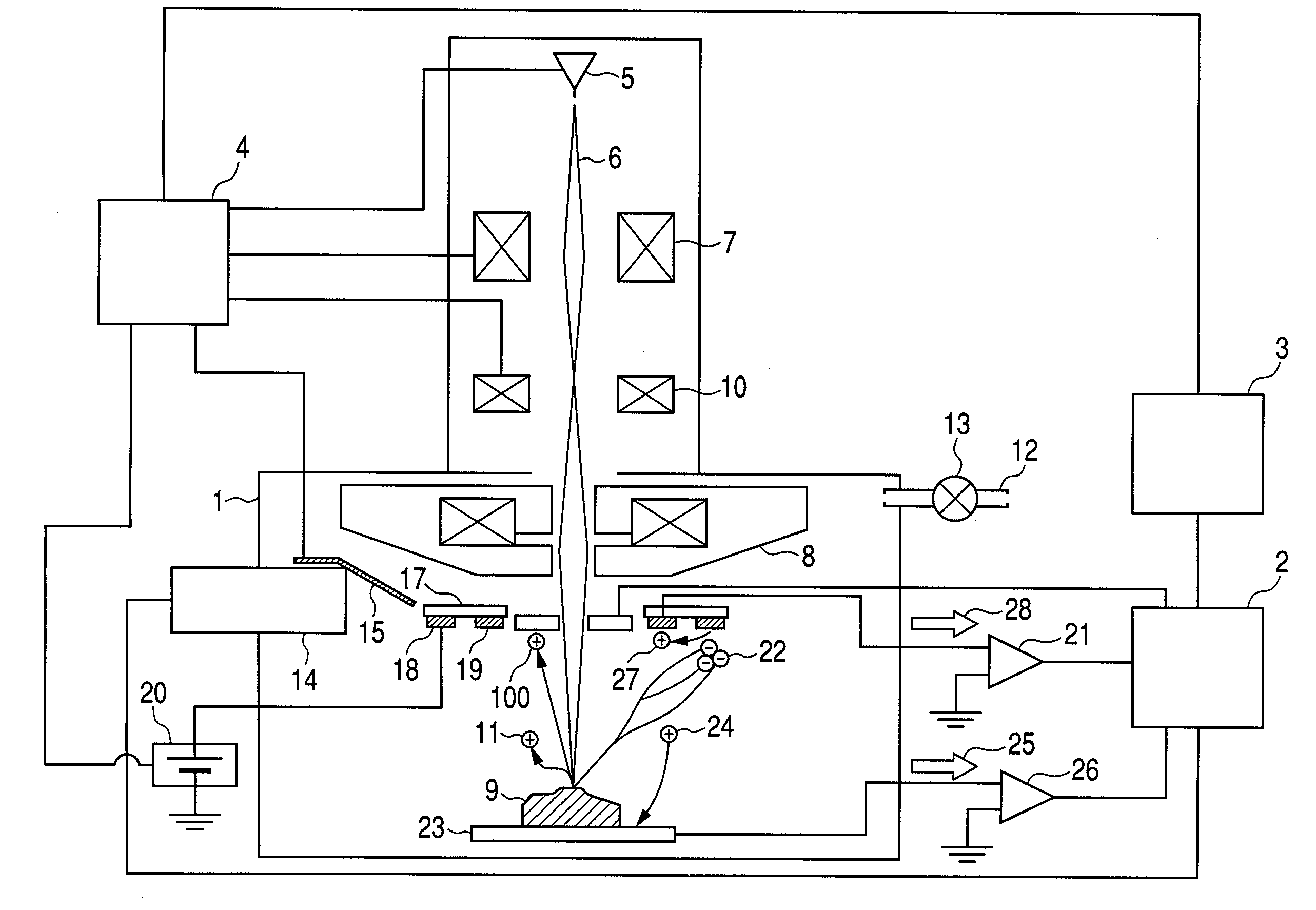
[0047]In a first embodiment, in a scanning electron microscope including a secondary electron detector formed on a flexible thin film type substrate as described above, the secondary electron detector that is arranged near an irradiation optical axis of a primary electron beam, that is, an on axial secondary electron detector will be described with respect to a first embodiment.
[0048]FIG. 1 schematically shows an outer appearance configuration of a scanning electron microscope in a type where an on axial secondary electron detector is arranged. The scanning electron microscope shown in FIG. 1 includes an electron optical lens tube including an objective lens 8, a sample chamber 1, an information processor 2 that performs a signal process on a positive current signal inducing a detected secondary electron and forms an image, and an image processing terminal 3 that is connected to the image processor, etc. The image processing terminal 3 includes a display unit that displays a formati...
second embodiment
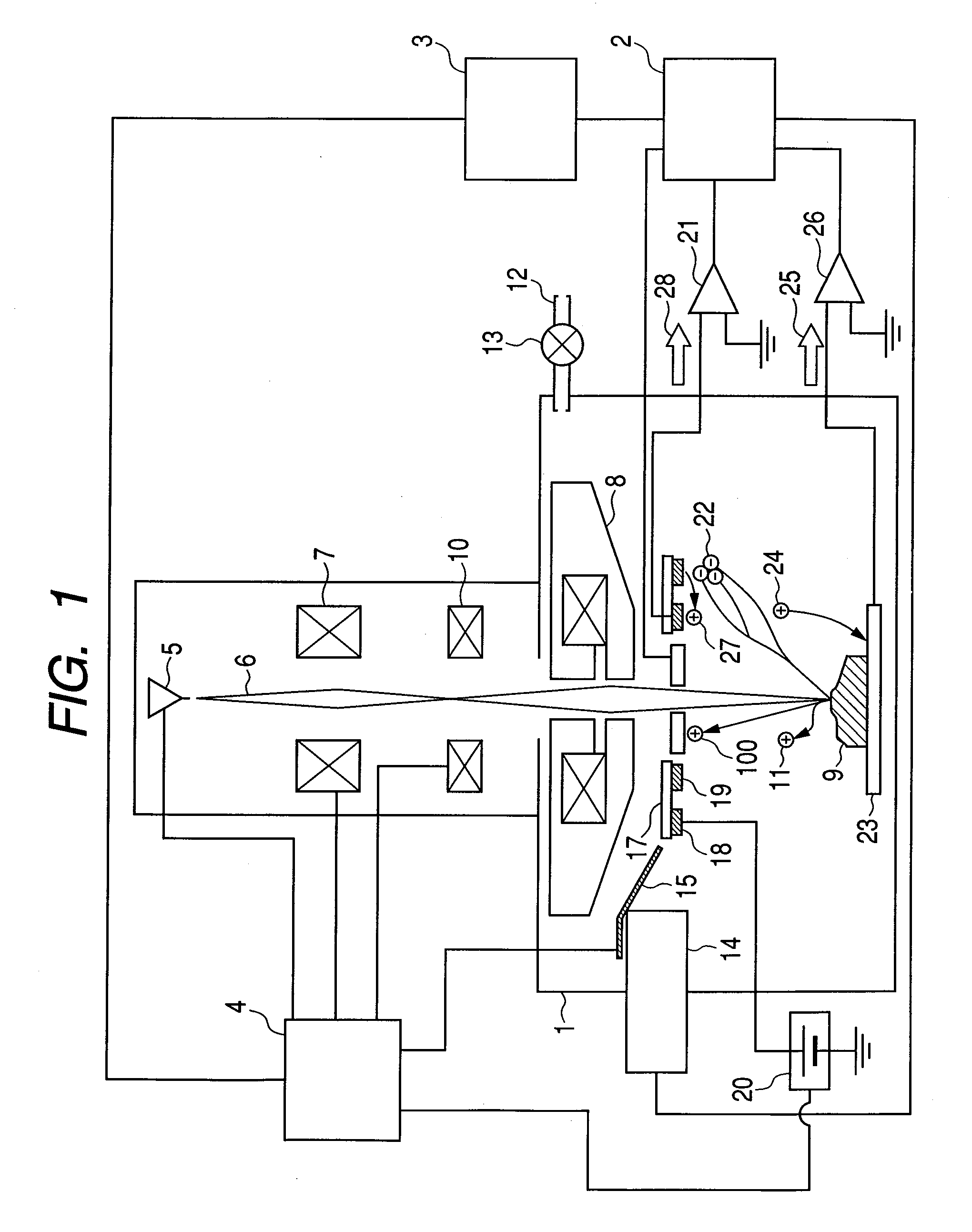
[0062]FIG. 3A shows another embodiment of the on axial secondary electron detector. The configuration other than the secondary electron detector is the same as the first embodiment. FIG. 3A is a pattern diagram showing the detector viewed from the sample direction. In the configuration of the electrode, the electric field supplying electrode 18 and the detection electrode 19 have a fan shape rather than a circular shape as compared to the first embodiment of the on axial secondary electron detector and a substrate 201 has a shape where a portion of the circle is chipped as compared to the substrate 14. As described above, there is an effect that the secondary electron detector does not shield the path of other detectors arranged at an off-axis such as an EDX detector and a high-vacuum secondary electron detector and the like and the sample by installing an area which does not include the substrate or the electrode. Further, even though the sample holder is inclined, the interference...
third embodiment
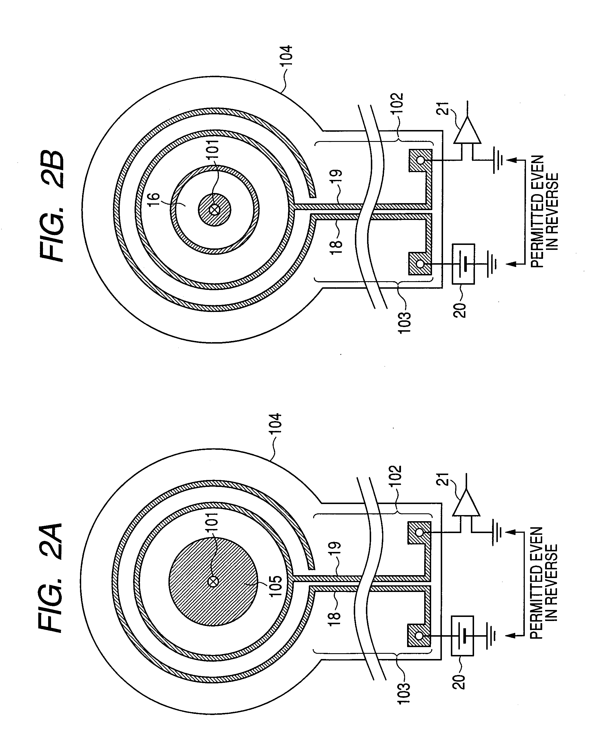
[0065]FIG. 4 shows a third embodiment of the on axial secondary electron detector. The configuration other than the secondary electron detector is the same as the first embodiment. FIG. 4 is a pattern diagram showing the detector viewed from the sample direction. In the electrode configuration of the third embodiment, the electric field supplying electrode 18 and the detection electrode 19 are shaped as a plurality of concentric doughnut types and alternately arranged to each other. As described above, an area, which amplifies the secondary electron, can be extended by forming pairs of the plurality of electric field supplying electrodes and the detection electrodes as compared to the first embodiment of the on axial secondary electron detector, the electron amplified therein moves to the outside thereof and can be amplified, the effect of the high-yield detection can be obtained. Further, even in the present configuration, the configuration of the fan shape of the second embodiment...
PUM
| Property | Measurement | Unit |
|---|---|---|
| energy | aaaaa | aaaaa |
| gas pressure | aaaaa | aaaaa |
| pressure | aaaaa | aaaaa |
Abstract
Description
Claims
Application Information