Lead-free solder alloy

a solder alloy and lead-free technology, applied in the direction of welding/cutting media/materials, manufacturing tools, welding apparatus, etc., can solve the problems of lead pollution of underground water caused by acid rain contact of printed wiring boards with acid rain, and achieve good impact resistance to drop and good solderability

Active Publication Date: 2009-09-17
SENJU METAL IND CO LTD
View PDF3 Cites 23 Cited by
  • Summary
  • Abstract
  • Description
  • Claims
  • Application Information

AI Technical Summary

Benefits of technology

[0018]An object of the present invention is to provide a lead-free solder alloy having good solde

Problems solved by technology

Wire bonding uses expensive gold wire, and even though operation is automated and performed at a high speed, electrodes are connected one by one, so the operation takes an extended period of time.
In addition, as the electrode density increases with an increase in the performance of chips, short circuits due to contact between wires has become unavoidable.
However, when printed wiring boards which are difficult to reuse are disposed of by burial, pollution of underground water with lead caused by contact of printed wiring boards with acid rain has become a problem.
For this reason the use of Pb-containing solder alloys has come to be restricted on a worldwide scale.
In general, the solderability of a Sn-based lead-free solder alloy is inferior compared to a conventional Sn—Pb based solder alloy.
Mobile electronic equipment can be subjected to impacts when dropped, and if soldered joints inside the electronic equipment break away as a result of such an impact, the equipment can no longer perform its intended function.
One of major causes of malfunctions when mobile electronic equipment is dropped is breakaway of

Method used


Image

  • Lead-free solder alloy
  • Lead-free solder alloy

Examples


examples

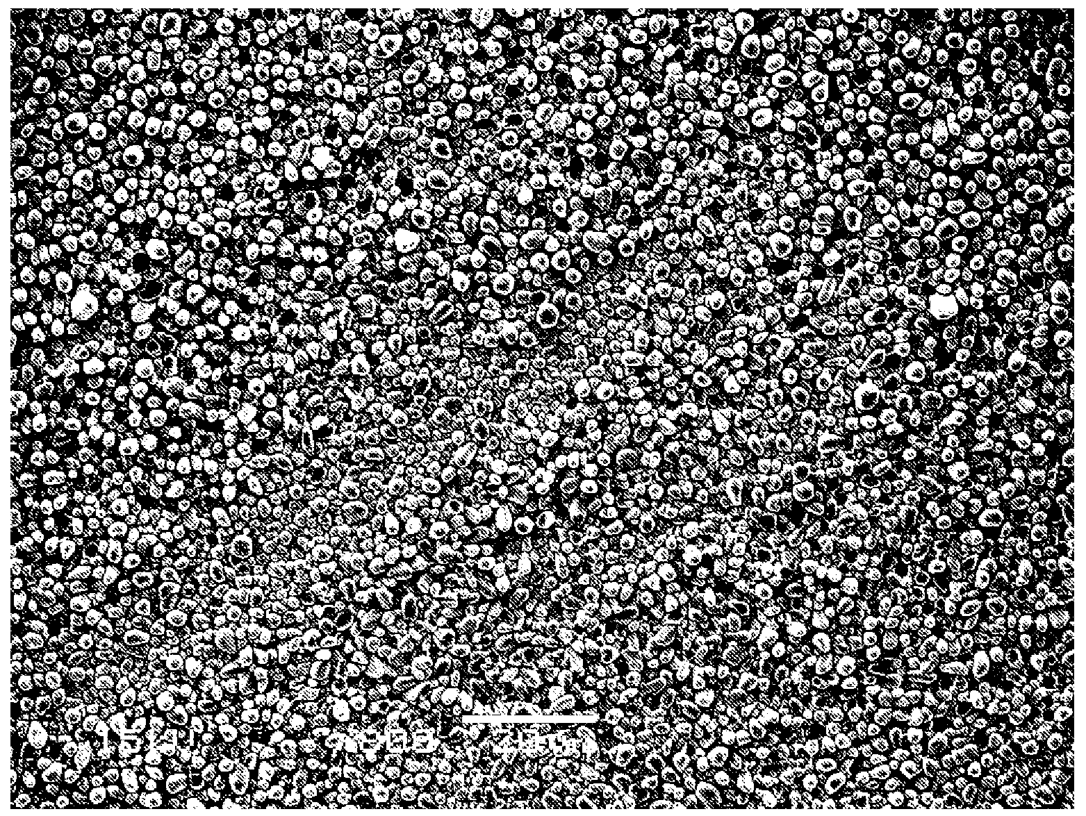
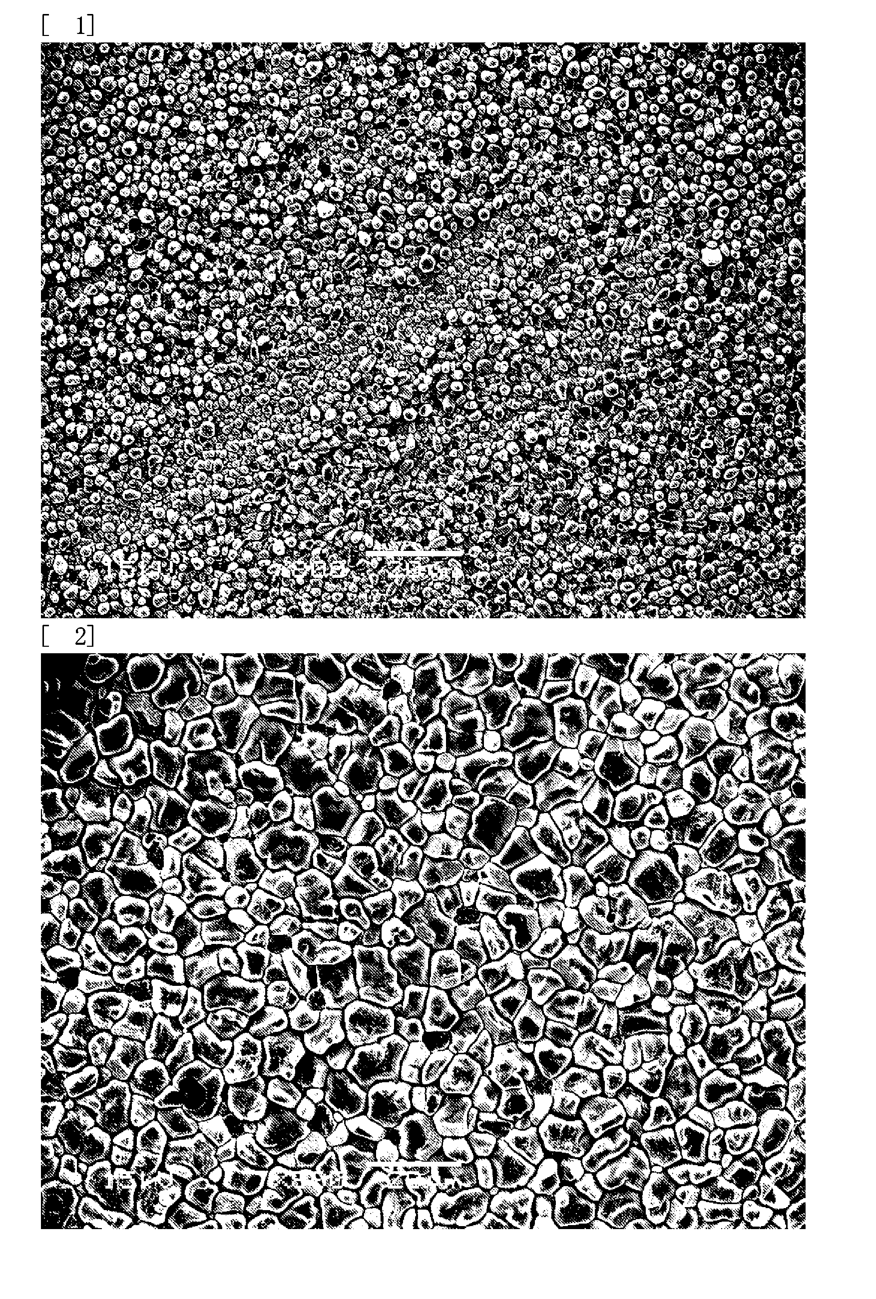
[0041]Solder balls having a diameter of 0.3 nun were prepared from the solder alloys having the compositions shown in Table 1. Among the solder alloys shown as comparative examples in Table 1, Comparative Examples 1 and 2 illustrate solder alloys having representative compositions described in Patent Documents 1 and 2, respectively. Comparative Examples 3 and 5 illustrate solder alloys described in Patent Document 3.

[0042]Using the solder balls, impact resistance to dropping before and after thermal aging, the thickness of an intermetallic layer measured after thermal aging, yellowing discoloration caused by heating, and the formation of voids were tested by the methods described below. The results are also shown in Table 1. Heating in a reflow furnace or a thermostatic oven in each test was carried out in air.

[0043][Impact Resistance to Dropping]

[0044](1) Flux is applied by printing to the electrodes of a CSP measuring 12×12 mm and having 192 electrodes (the surfaces of which were ...


PUM

PropertyMeasurementUnit
Fractionaaaaaaaaaa
Fractionaaaaaaaaaa
Fractionaaaaaaaaaa

Abstract

A lead-free solder alloy is provided which has improved impact resistance to dropping even after thermal aging and which is excellent with respect to solderability, occurrence of voids, and yellowing. A solder alloy according to the present invention consists essentially of, in mass percent, (1) Ag: 0.8-2.0%, (2) Cu: 0.05-0.3%, (3) at least one element selected from In: at least 0.01% and less than 0.1%, Ni; 0.01-0.04%, Co: 0.01-0.05%, and Pt: 0.01-0.1%, optionally (4) at least one element selected from Sb, Bi, Fe, Al, Zn, and P in a total amount of up to 0.1%, and a remainder of Sn and impurities.

Description

TECHNICAL FIELD[0001]This invention relates to a lead-free solder alloy containing no lead and particularly to a lead-free solder alloy which is suitable for forming minute solder portions such as solder bumps.BACKGROUND ART[0002]Mounting of extremely small multifunctional semiconductor packages such as a BOA (ball grid array) and CSP (chip size package) on printed wiring boards is often carried out by means of solder bumps. When carrying out such mounting, solder bumps are previously formed atop the electrodes of a package, and the package is disposed so that the solder bumps contact the portions to be soldered (lands) of a printed wiring board. The printed wiring board and the package are then heated in a heating apparatus such as a reflow furnace and the bumps are melted to solder the package to the printed wiring board and to provide electrical continuity between the two member.[0003]Solder bumps are also utilized for mounting of a bare chip to a printed wiring board. Such mount...

Claims


Application Information

Patent Timeline
IPC IPC(8): C22C13/02C22C13/00
CPCB23K35/262H05K3/3463C22C13/00
Inventor OHNISHI, TSUKASAYAMAKI, TOKUROSOMA, DAISUKE
Owner SENJU METAL IND CO LTD
Why Eureka
Try Eureka