Linewidth measuring method, image-forming-state detecting method, adjustment method, exposure method, and device manufacturing method

a technology of image-forming state and measurement method, applied in the direction of material analysis by optical means, instruments, photomechanical devices, etc., can solve the problems of difficult to directly obtain the pattern shape, long measurement time per point, and difficulty in performing the measurement at a plurality of points, etc., to achieve the effect of improving the productivity (including the yield) of microdevices, low cost and high throughpu

Inactive Publication Date: 2009-09-17
NIKON CORP
View PDF9 Cites 7 Cited by
  • Summary
  • Abstract
  • Description
  • Claims
  • Application Information

AI Technical Summary

Benefits of technology

[0024]With this method, the linewidth of the image of the pattern formed on the object by exposure is measured with low cost and high throughput in one of the first and second linewidth measuring methods of the present invention, and based on the measured linewidth, exposure conditions of the object are determined. Accordingly, high-precision exposure of the object is realized.
[0025]In the lithography process, the productivity (including the yield) of microdevices can be improved by exposing the object in any one of the first to third exposure methods of the present invention. Consequently, according to an eighth aspect of the present invention, it can also be said that there is provided a device manufacturing method, including a lithography process in which an object is exposed in one of the first and second exposure methods of the present invention.

Problems solved by technology

In the OCD measurement, an incident light is irradiated to a one-dimensional-grating-shaped pattern that has a periodic structure of line-and-space, and a pattern shape is obtained by analyzing a wavelength property and an incident angle property of the diffracted light, but it is difficult to directly obtain the pattern shape (e.g. linewidth) from measurement information (e.g. spectral information of interference fringes generated by interference of diffracted lights from the grating-shaped pattern, or the like), and therefore a library method is frequently used.
However, in the method in which the linewidth of a resist image is directly measured with the SEM, since the focusing of the SEM needs to be performed precisely, the measurement time per point is very long, and therefore several hours to several tens of hours are required for performing the measurement at a plurality of points.
Further, while a high-speed measurement can be performed in the electric dimension measurement method described above, this measurement method has high running cots because costly special wafers need to be used and also a device to perform etching of the wafers becomes necessary.
Accordingly, in the case of performing high-precision measurement, the number of the models owned as the library has to be increased, and therefore much time is required for preparing the library, and also the measurement time gets longer according to the increase of the number of the models, which decreases the throughput.

Method used


Image

  • Linewidth measuring method, image-forming-state detecting method, adjustment method, exposure method, and device manufacturing method
  • Linewidth measuring method, image-forming-state detecting method, adjustment method, exposure method, and device manufacturing method
  • Linewidth measuring method, image-forming-state detecting method, adjustment method, exposure method, and device manufacturing method

Examples


Embodiment Construction

[0040]An embodiment of the present invention is described below, referring to FIGS. 1 to 11.

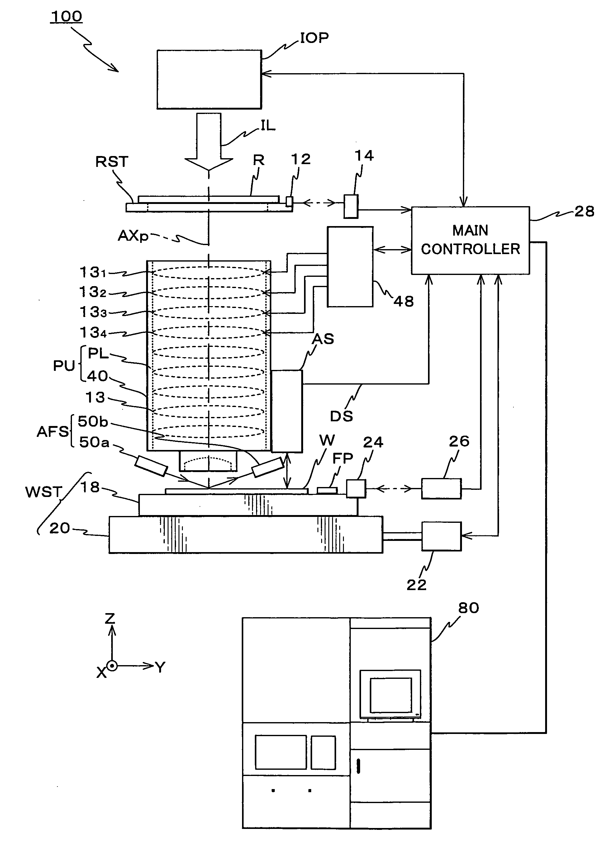
[0041]FIG. 1 shows a schematic configuration of an exposure apparatus 100 related to the embodiment. Exposure apparatus 100 is a reduction projection exposure apparatus by a step-and-scan method (a so-called scanning stepper (which is also called a scanner)). In the description below, the explanation is given assuming that a direction parallel to an optical axis AXp of a projection optical system PL (to be described later) is a Z-axis direction, a direction in which a reticle and a wafer are relatively scanned within a plane orthogonal to the Z-axis direction is a Y-axis direction, and a direction that is orthogonal to a Z-axis and a Y-axis is an X-axis direction, and rotation (inclination) directions about an X-axis, the Y-axis and the Z-axis are θx, θy and θz directions, respectively.

[0042]Exposure apparatus 100 is equipped with an illumination system IOP, a reticle stage RST that holds a r...


PUM

PropertyMeasurementUnit
output wavelengthaaaaaaaaaa
lengthaaaaaaaaaa

Abstract

A pattern area that includes a plurality of line patterns with a predetermined spacing therebetween formed on a wafer is imaged, and based on the imaging results, a contrast value of an image of the pattern area is computed, and the computed contrast value is converted into the linewidth of the line pattern based on known conversion information. Therefore, even if the pattern area is imaged using a microscope having a low resolving power, e.g. an image-forming type alignment sensor or the like, without using the SEM, the linewidth of the line pattern can be measured with high precision. Accordingly, linewidth measurement with low cost and high throughput becomes possible.

Description

CROSS-REFERENCE TO RELATED APPLICATIONS[0001]This application is a continuation of International Application PCT / JP2007 / 068930, with an international filing date of Sep. 28, 2007, the disclosure of which is hereby incorporated herein by reference in its entirety, which was not published in English.BACKGROUND OF THE INVENTION[0002]1. Field of the Invention[0003]The present invention relates to linewidth measuring methods, image-forming-state detecting methods, adjustment methods, exposure methods and device manufacturing methods, and more particularly, to a linewidth measuring method in which a linewidth of a pattern formed on an object is measured, an image-forming-state detecting method in which based on a measurement result obtained by measuring the linewidth of the pattern formed on the object via an optical system using the linewidth measuring method, a forming state of an image of a pattern including the pattern previously referred to is detected, an adjustment method in which ...

Claims


Application Information

Patent Timeline
Patent Type & Authority Applications(United States)
IPC IPC(8): G03F7/20G01B11/02G01N21/00
CPCG03F7/70625G03F7/70191G03F7/7055G03F7/70558
Inventor MIYASHITA, KAZUYUKI
Owner NIKON CORP
Why Eureka
Try Eureka