Integrated Reed Switch

a reed switch and integrated technology, applied in selector switches, relays, contacts, etc., can solve the problems of low sensitivity, low sensitivity, and low sensitivity of reed switches, so as to reduce size and maintain sensitivity , the effect of reducing the siz

Active Publication Date: 2009-09-24
HT MICROANALYTICAL +1
View PDF25 Cites 11 Cited by
  • Summary
  • Abstract
  • Description
  • Claims
  • Application Information

AI Technical Summary

Benefits of technology

[0012]The functional device, economic, and fabrication constraints for a microfabricated reed switch as briefly discussed above encourage planar fabrication that can support structure definition extending considerably (100s of micrometers) out of the plane of the manufacturing substrate. This type of processing can be referred to as “high aspect-ratio” processing where the thickness out of the processing plane of a device feature can be much larger than corresponding lateral or in-plane dimensions. This allows offsetting of some of the detriments of the volume scaling of a reed switch if it is fabricated with its compliant direction in the plane of the substrate since the width of the reed blades (height above the substrate) can be made several hundred micrometers. At the same

Problems solved by technology

Conventional glass encapsulated reed switches are produced by a relatively inaccurate stamping process which leads to poor thickness control and thu

Method used


Image

  • Integrated Reed Switch
  • Integrated Reed Switch
  • Integrated Reed Switch

Examples


example reed switch embodiments

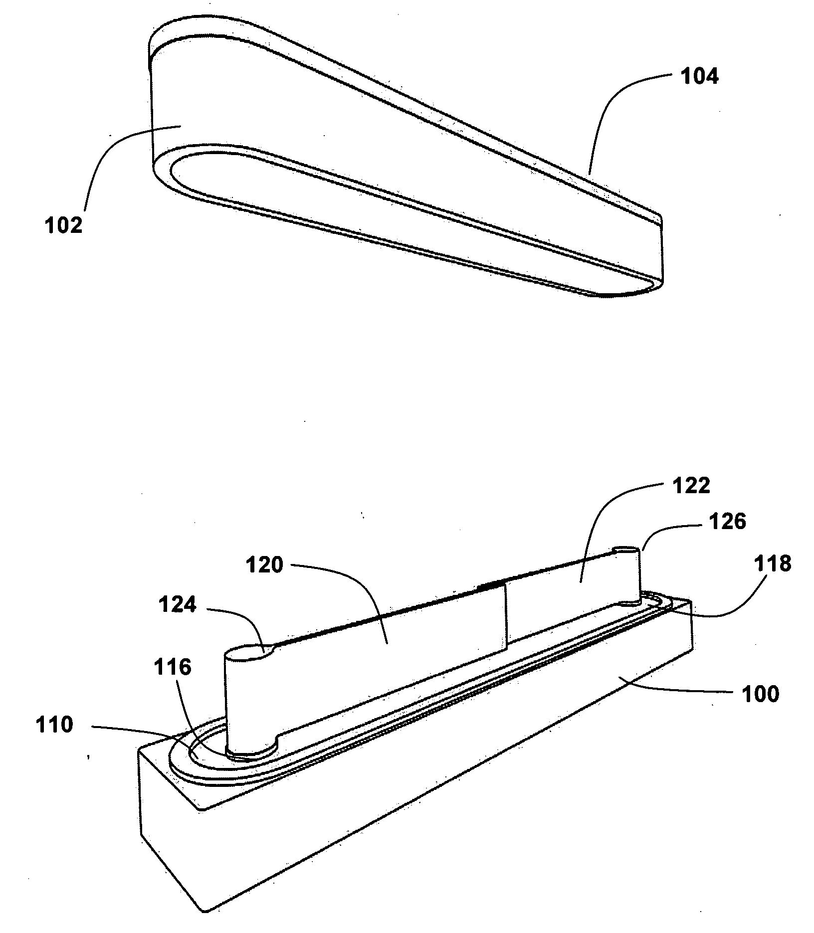
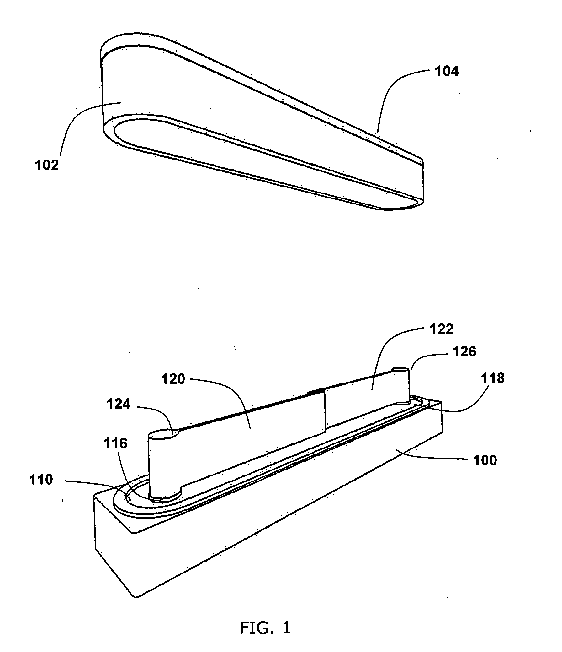
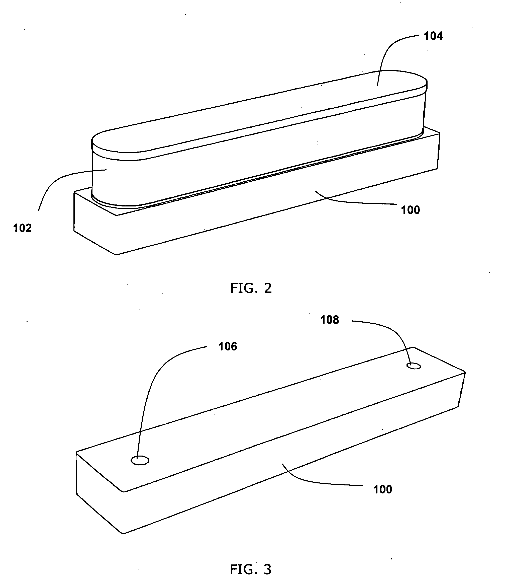
[0042]Example embodiments of a microfabricated reed switch according to the present invention can comprise an electrically insulating substrate provided with electrical vias or feedthroughs, a reed switch mechanism, a cover to provide hermetic sealing of the reed switch, and electrically conducting pads to provide electrical connection to the reed switch. The figures generally show only a single example switch, comprising only a dice portion of a wafer or die pertaining to a single switch device. In production, many such switches (or other devices) can be fabricated on a single substrate.

[0043]FIG. 1 is an exploded view of an example integrated single pole—single throw (“SPST” or “form A”) integrated reed switch. FIG. 2 is a view of the example switch of FIG. 1 sealed, packaged and singulated. A substrate 100 has electrical vias 106, 108 as shown in the view of the example switch in FIG. 3. The substrate can comprise any of a variety of electrically insulating materials, as examples...

example method

of Making

[0053]A description of fabrication of an integrated reed switch according to the present invention can begin with preparation of a suitable substrate. A variety of insulating substrates such as alumina, glass, glass-ceramic composite and oxidized silicon can be used. Electrical connection to the reed switch can be provided by vias, formed in holes, which can range in size with diameters of 0.002″ to 0.040″ for some applications. Such holes can be machined using laser or water jet drilling. The holes can be provided with electrically conductive material by a number of approaches. The selection of an approach can affect a level of hermeticity acceptable to reed switch longevity for the intended application. As examples, the holes can be provided with electrically conductive material by using thin film physical vapor deposition combined with electroplating or by using pressed, sintered, and fired metal powders or conductive plug paste in a ceramic slurry type of process. Suita...

example embodiment

with Sidewall and Cap

[0059]FIG. 24 and 25 are perspective views of an example embodiment of a reed switch with sidewalls 1001 and a cap 1000. Other example embodiments described herein comprise a cap having two layers: a planar layer and a sidewall layer, such that the sidewall is mounted with the reed switch and positioned within the planar layer above the switch elements. In the example embodiments of FIGS. 24 and 25, a sidewall layer 1001 is formed as part of the switch fabrication process. The cap can then comprise a layer 1002, e.g., of a dielectric or metal material, that mounts with the sidewalls 1001 previously created as part of the switch through the use of a relatively thin spacing pattern 1003. This approach provides a wafer level bonded substrate sandwich for which the cap can be created during singulation or wafer dicing (instead of lithographically).


PUM

PropertyMeasurementUnit
Thicknessaaaaaaaaaa
Electrical conductivityaaaaaaaaaa
Magnetic fieldaaaaaaaaaa

Abstract

This invention relates to reed switches, and more particularly to micro-miniaturized reed switches and batch microfabrication techniques used to fabricate micro-miniaturized reed switches. The present invention can provide miniaturized reed switches with more consistent operating parameters, and that can be produced more efficiently than conventional reed switches. The present invention can also provide methods of making miniaturized reed switches using microfabrication techniques. The present invention can use lithographic-based fabrication to enable monolithic construction of a reed switch. Microlithography can repeatedly form micrometer dimensions with tight tolerances over large arrays of devices which, if the patterns are translated into materials appropriate for electromechanical devices, can provide for repeatable and consistent electromechanical operation. For example, tight dimensional control of the gap between two reeds in a reed switch or a reed and a fixed contact can provide consistency of performance between reed switches. Thus, the present invention can allow the commonly regarded reed switch specification of sensitivity, or “Ampere-turns” required to close a reed switch, to be tightly controlled with a commensurate reduction in spread in sensitivity across reed switch production lots.

Description

CROSS-REFERENCE TO RELATED APPLICATIONS[0001]This application claims priority to U.S. provisional application 61 / 038,340, filed Mar. 20, 2008, which is incorporated herein by reference.FIELD OF THE INVENTION[0002]This invention relates to reed switches, and more particularly to micro-miniaturized reed switches and batch microfabrication techniques used to fabricate micro-miniaturized reed switches.BACKGROUND[0003]Dry reed switches are commonly comprised of two overlapping soft ferromagnetic electrically conducting cantilevers (reeds) separated by a small gap and supported by a glass hermetic enclosure. Upon application of a magnetic field the two opposing cantilevers are attracted to each other and establish electrical contact between the reeds. In the absence of a magnetic field the cantilevers resort to their original separated and electrically insulating state. Numerous electromechanical and electrical variations of this basic “single-pole, single-throw” normally open switch are ...

Claims


Application Information

Patent Timeline
IPC IPC(8): H01H1/66
CPCY10T29/49105H01H1/66
Inventor CHRISTENSON, TODD R.
Owner HT MICROANALYTICAL
Why Eureka
Try Eureka