Sonos device with insulating storage layer and p-n junction isolation

a technology of p-n junction isolation and insulating storage layer, which is applied in the field of semiconductor devices, can solve the problems of difficult fine bit lines b>30/b>, only having an opening in the ono film, etc., and achieves the effect of reducing the contact resistan

Active Publication Date: 2009-09-24
MONTEREY RES LLC
View PDF5 Cites 5 Cited by
  • Summary
  • Abstract
  • Description
  • Claims
  • Application Information

AI Technical Summary

Benefits of technology

[0016]Yet another embodiment of the claimed subject matter provides a method for manufacturing a semiconductor device comprising: forming a third silicon nitride film on a semiconductor substrate; forming bit lines in the semiconductor substrate by using a mask layer formed on the third silicon nitride film as a mask; forming a spacer on a side of the mask layer; removing the third silicon nitride film by using the mask layer and the spacer as a mask; and forming a metal silicide layer on each of the bit lines by using the third silicon nitride film as a mask. According to the present invention, since the edges of the bit lines and the silicide metal layer are offset, the silicide metal layer can be prevented from being formed on the semiconductor substrate.
[0017]According to the present invention, the semiconductor device which prevents electric charges stored in the ONO film from diffusing onto the bit lines or reduces the contact resistance between the bit lines and the plug metal, and the method for manufacturing the same is provided.

Problems solved by technology

Unfortunately, disposing an opening only in the ONO film 20a on the fine bit line 30 can be difficult.

Method used


Image

  • Sonos device with insulating storage layer and p-n junction isolation
  • Sonos device with insulating storage layer and p-n junction isolation
  • Sonos device with insulating storage layer and p-n junction isolation

Examples


first embodiment

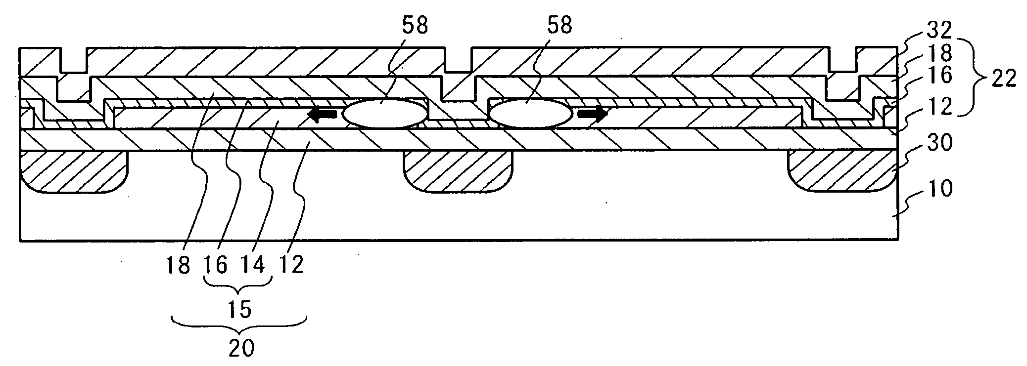
[0104]FIG. 13 is an illustration equivalent to the cross-sectional view taken along the line A-A in FIG. 12A of the flash memory of the The bit line 30 is disposed in the semiconductor substrate 10. The first ONO film 20 is disposed on the semiconductor substrate 10 between the bit lines 30, and the second ONO film 22 is disposed on the bit line 30. The film thickness of the first silicon nitride film 15 in the first ONO film 20 is larger than the film thickness of the second silicon nitride film 16 in the second ONO film 22. Therefore, the diffusion of electric charges 58 stored in the thick first silicon nitride film 15 in the neighborhood of the bit line 30 towards the thin second silicon nitride film 16 on the bit line 30 can be prevented. Furthermore, in FIG. 6B, when forming the second silicon oxide film 18, the upper silicon nitride film 16 is disposed on the bit line 30. Therefore, the upper silicon nitride film 16 prevents oxygen from diffusing and prevents the bit line 30...

second embodiment

[0126]According to one embodiment, as shown as t0 in FIG. 12C, edges of the bit line 30 and the metal silicide layer 36 only have an offset of no more than the amount of diffusion of the bit line 30 in a horizontal direction. In this case, there is a possibility of the metal silicide layer 36 also being formed on the p-type semiconductor substrate 10. since the edges of the bit line 30 and the metal silicide layer 36 are offset, it is possible to prevent the metal silicide layer 36 from being formed on the p-type semiconductor substrate 10.

[0127]Subsequently, as shown in FIGS. 18A to 18C, the second silicon oxide film 18 is formed on the third silicon nitride film 15a between the bit lines 30 and on the bit line 30 where the third silicon nitride film 15a and the first silicon oxide film 12 have been removed. As shown in FIGS. 19A to 19D, on the second silicon oxide film 18, the word line 32 is formed crossing the bit line 30. As shown in FIGS. 21A to 21D, the second silicon oxide ...


PUM


Abstract

The present invention provides a semiconductor device and a method for manufacturing thereof. The semiconductor device includes bit lines disposed in a semiconductor substrate, a first ONO disposed between the bit lines on the semiconductor substrate, and a second ONO film disposed on each of the bit lines. The film thickness of a first silicon nitride film in the first ONO film is larger than the film thickness of a second silicon nitride film in the second ONO film.

Description

CLAIM OF PRIORITY[0001]This application claims priority from Japanese patent application 2007-243952 filed on Sep. 20, 2007.TECHNICAL FIELD[0002]The present invention relates to a semiconductor device and a method for manufacturing the same and, more particularly, to a semiconductor device having a non-volatile memory disposed with a bit line and an ONO film and a method for manufacturing the same.BACKGROUND[0003]Recently, the usage of non-volatile memory comprising a semiconductor device capable of rewriting data and retaining data stored therein even while the device is un-powered has become increasingly popular. Flash memory is one example of non-volatile memory. A typical flash memory is disposed with a transistor which operates as a memory cell and includes a floating gate or an insulating film called a charge storage layer for accumulating electrons used to store data. Flash memory with a SONOS (Silicon Oxide Nitride Oxide Silicon) structure for accumulating the electrons in a...

Claims


Application Information

Patent Timeline
Patent Type & Authority Applications(United States)
IPC IPC(8): G11C16/04H01L29/792H01L21/336G11C11/34
CPCH01L27/11568H01L27/11565H10B43/10H10B43/30
Inventor MURAI, HIROSHIHIGASHI, MASAHIKO
Owner MONTEREY RES LLC
Why Eureka
Try Eureka