Photoelectric conversion device and method for manufacturing the same

a conversion device and photoelectric technology, applied in the field of photoelectric conversion devices and methods for manufacturing the same, can solve the problems of reducing the bonding strength, the degree of adhesion in the adhesion portion or the change in the property of the electrode-forming paste serving as an adhesive becomes a problem, and the number and complexity of manufacturing steps or process temperatures are limited, so as to achieve resource-saving photoelectric conversion, the effect of reducing the amount of a single crystal semiconductor material and reducing the amount o

Inactive Publication Date: 2009-10-01
SEMICON ENERGY LAB CO LTD
View PDF17 Cites 45 Cited by
  • Summary
  • Abstract
  • Description
  • Claims
  • Application Information

AI Technical Summary

Benefits of technology

[0011]In view of the foregoing problems, it is an object of the present invention to provide a method for manufacturing a photoelectric conversion device with excellent photoelectric conversion characteristics through a simple process. Further, it is another object of the present invention to provide a resource-saving photoelectric conversion device in which a resource such as a semiconductor material is effectively utilized and to provide a method for manufacturing the photoelectric conversion device. Furthermore, it is another object of the present invention to provide a photoelectric conversion device typified by a solar cell with an excellent photoelectric conversion characteristic and to provide a method for manufacturing the photoelectric conversion device.
[0033]A photoelectric conversion device is manufactured using detached thin part of a single crystal semiconductor substrate; accordingly, the amount of a single crystal semiconductor material used can be reduced more than before, and thus, a resource-saving photoelectric conversion device can be provided. The rest of the single crystal semiconductor substrate from which thin part of a single crystal semiconductor substrate as a raw material has been detached can be repeatedly reused, and thus, a resource can be effectively utilized.
[0034]Further, by forming a stack-type photoelectric conversion device in which a unit cell having a non-single-crystal semiconductor layer is stacked over a unit cell having detached thin part of a single crystal semiconductor substrate, a photoelectric conversion device with an excellent photoelectric conversion characteristic can be provided. Furthermore, when a semiconductor layer including a non-single-crystal semiconductor layer is formed over a detached thin single crystal semiconductor layer by a chemical vapor deposition method, typically a plasma CVD method to manufacture a stack-type photoelectric conversion device, a photoelectric conversion device with an excellent photoelectric conversion characteristic can be manufactured through a simple process.

Problems solved by technology

However, in a method like Patent Document 1 in which a single crystal silicon substrate is bonded to another substrate with electrode-forming paste as an adhesive, the degree of adhesion in an adhering portion or the change in property (the reduction in bonding strength) of the electrode-forming paste serving as an adhesive becomes a problem.
Further, bonding to another substrate may cause increase in the number and complexity of manufacturing steps or limitation on a process temperature due to a property of a material for the substrate to be bonded.
Therefore, even if high efficiency is achieved, problems such as increase in cost, reduction in productivity, and unsuitability for mass production due to increase in complexity of manufacturing steps or the like still remain.
Consequently, there is a concern that power generated by a photoelectric conversion device having such problems cannot compete with a conventional commercial power.

Method used


Image

  • Photoelectric conversion device and method for manufacturing the same
  • Photoelectric conversion device and method for manufacturing the same
  • Photoelectric conversion device and method for manufacturing the same

Examples


embodiment 1

[0055]In this embodiment, a method for manufacturing a photoelectric conversion device and a structure of the manufactured photoelectric conversion device, are described with reference to drawings. In the photoelectric conversion device in this embodiment, a bottom cell is formed using a thin single crystal semiconductor layer obtained by detaching thin part of a single crystal semiconductor substrate and a top cell is formed in which a non-single-crystal semiconductor layer is present over the thin single crystal semiconductor layer.

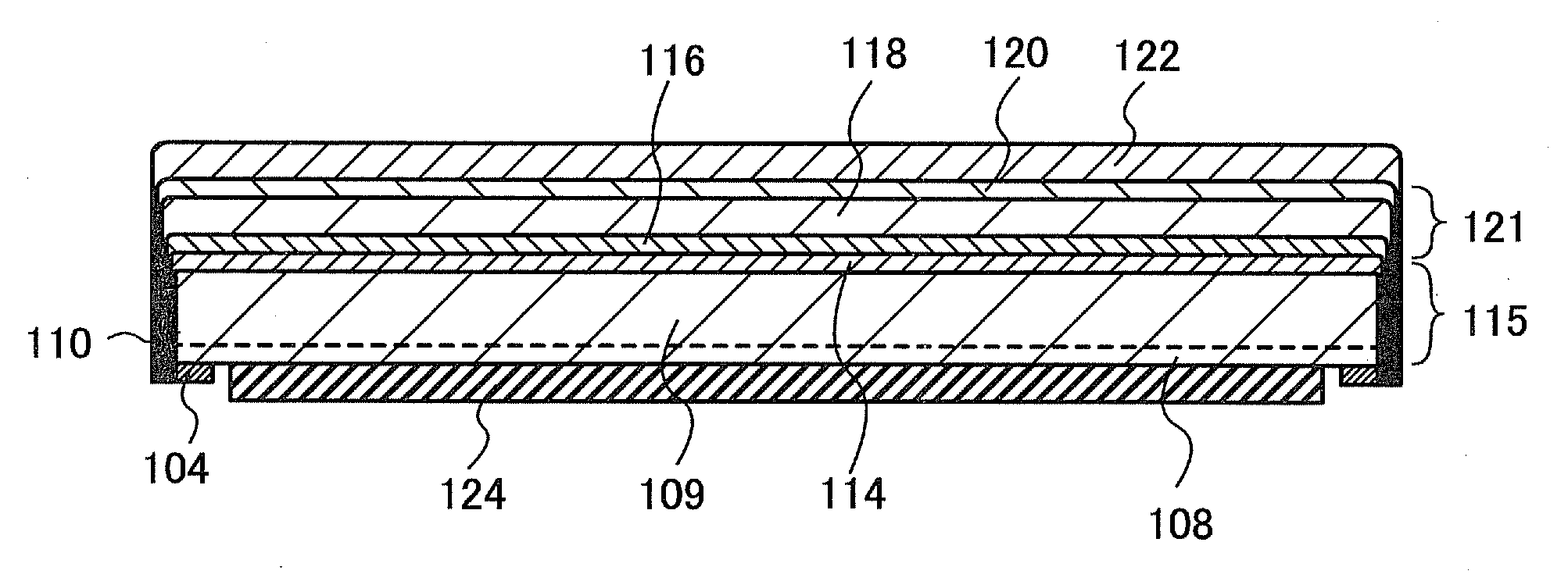
[0056]FIG. 1 shows an example of a cross-sectional view of a photoelectric conversion device according to the present invention.

[0057]A photoelectric conversion device described in this embodiment is provided with a stacked structure of a first unit cell 115 having a single crystal semiconductor layer and a second unit cell 121 having a non-single-crystal semiconductor layer. The stacked structure of the first unit cell 115 and the second unit cell 121 ...

embodiment 2

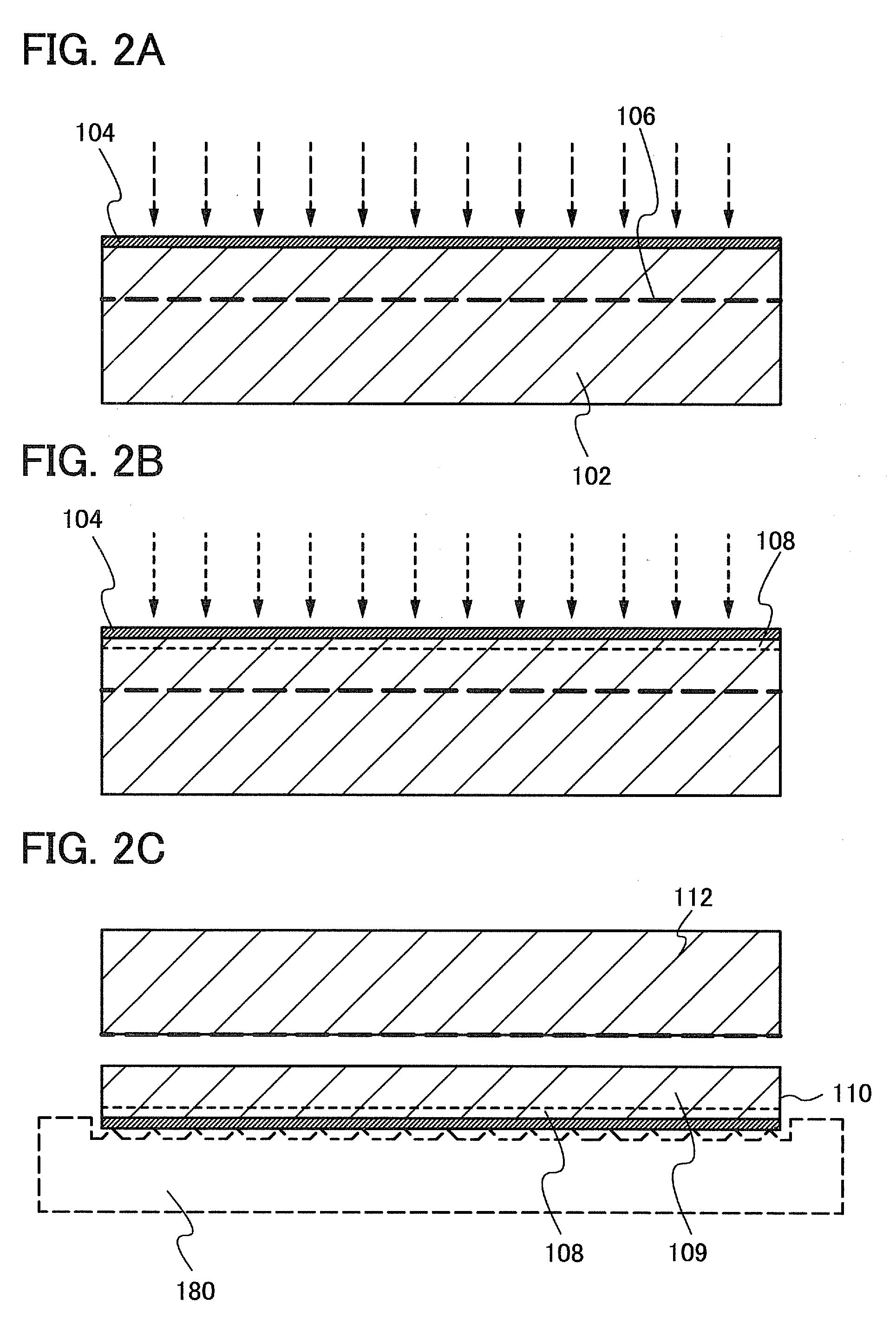
[0134]In this embodiment, an example of a method for manufacturing a photoelectric conversion device which is different from that described in the above embodiment will be described. Specifically, a method for forming a modified region in a single crystal semiconductor substrate as an embrittled layer by utilizing multiphoton absorption is described. Note that the same portions as in the above embodiment are denoted by the same reference numerals, and explanation thereof will be omitted or partially simplified.

[0135]In Embodiment 1, a mode is described with reference to FIG. 2A in which the embrittled layer 106 is formed in the single crystal semiconductor substrate 102 at a predetermined depth by irradiation with ions (typically hydrogen ions) accelerated by voltage and then the single crystal semiconductor substrate 102 is divided at the embrittled layer 106 by heat treatment to obtain the thin single crystal semiconductor layer 110, which is detached thin part of a single crystal...

embodiment 3

[0162]In this embodiment, an example of a structure of a photoelectric conversion device which is different from that in the above embodiments and a method for manufacturing the photoelectric conversion device having the structure will be described. Specifically, a structure is described in which a surface is provided with an anti-reflection structure (a structure of depressions and projections). Further, in this embodiment, an example is described in which a single crystalline silicon substrate is used as the single crystal semiconductor substrate 102. Note that the description of a portion which overlaps with the above embodiments is omitted or partially simplified.

[0163]As shown in FIG. 8A, surfaces of a single crystal silicon substrate 1002 are etched utilizing the fact that silicon is etched using an alkaline solution at different etching rates according to the orientation of crystal planes. By the etching, minute depressions and projections are formed in the surfaces of the si...


PUM


Abstract

To provide a resource-saving photoelectric conversion device with excellent photoelectric conversion characteristics. Thin part of a single crystal semiconductor substrate, typically a single crystal silicon substrate, is detached to structure a photoelectric conversion device using a thin single crystal semiconductor layer, which is the detached thin part of the single crystal semiconductor substrate. The thin part of the single crystal semiconductor substrate is detached by a method in which a substrate is irradiated with ions accelerated by voltage, or a method in which a substrate is irradiated with a laser beam which makes multiphoton absorption occur. A so-called tandem-type photoelectric conversion device is obtained by stacking a unit cell including a non-single-crystal semiconductor layer over the detached thin part of the single crystal semiconductor substrate.

Description

BACKGROUND OF THE INVENTION[0001]1. Field of the Invention[0002]The present invention relates to a photoelectric conversion device using a single crystal semiconductor or a polycrystalline semiconductor and to a method for manufacturing the photoelectric conversion device.[0003]2. Description of the Related Art[0004]Since the situation of global warming has been serious, a measure against the global warming is an issue that needs to be addressed worldwide. Most greenhouse effect gases which are regarded as a main cause for global-warming, such as carbon dioxide, are exhausted by consumption of energy, such as oil, coals, and natural gases. However, such energy is indispensable to the industrial society. Therefore, the amount of energy consumption cannot be reduced simply. Thus, solar-electric power generation which discharges less amount of carbon dioxide and which is eco-friendly has attracted attentions as the next-generation energy.[0005]For the solar-electric power generation, a...

Claims


Application Information

Patent Timeline
Patent Type & Authority Applications(United States)
IPC IPC(8): H01L31/00H01L21/78H01L31/06H01L31/078H01L31/18
CPCH01L31/022425H01L31/1804H01L31/03921H01L31/068H01L31/0687H01L31/072H01L31/0725H01L31/075H01L31/076Y02E10/544Y02E10/548Y02E10/547H01L31/182H01L31/1896H01L31/18H01L31/0236H01L21/76254H01L31/02363Y02P70/50
Inventor YAMAZAKI, SHUNPEISHIMOMURA, AKIHISA
Owner SEMICON ENERGY LAB CO LTD
Why Eureka
Try Eureka