Method for mounting semiconductor device, as well as circuit board, electrooptic device, and electronic device

a technology of conductive bonding material and semiconductor device, which is applied in the direction of identification means, paper/cardboard containers, instruments, etc., can solve the problems of reducing coupling reliability, difficult mounting of driver ic using conductive bonding material, and increasing the size of conductive particles contained in the above conductive bonding material such as acf and acp, so as to achieve the effect of improving coupling reliability

Inactive Publication Date: 2009-10-01
SEIKO EPSON CORP
View PDF11 Cites 2 Cited by
  • Summary
  • Abstract
  • Description
  • Claims
  • Application Information

AI Technical Summary

Benefits of technology

[0012]With such a configuration, wherein hot pressing is conducted within a temperature range including the glass transition temperature of the resin, the elastic modulus of the convexity formed of resin starts to decrease at a temperature for bonding the semiconductor device on the substrate. Thus, an external electrode comprising the convexity of the semiconductor makes a transformation during the hot pressing conducted at the time of bonding, thereby assuring coupling with the electrode terminal on the substrate. As a result, the problem of poor conduction can be solved and the coupling reliability can be improved. Further, the availability of NCP coupling eliminates the need of using a bonding material containing anisotropic conductive particles, which leads to a cost reduction. Also, the manufacturing of a convexity using a resin having a high elastic modulus at a room temperature becomes possible. As a result, the choice of resin materials is widened and therefore cost reduction can be achieved by using an inexpensive resin. Furthermore, by using the above-described resin as a material for the convexity, the elastic modulus of the resin decreases at the time of bonding and therefore bonding at a low load (force) becomes possible. Thus, the formation of a convexity on a region where there is a switching element or the like becomes possible. This means that an electrode can be formed on any region of a semiconductor device whether or not there is a switching element present. Moreover, in the case where the convexity is formed on a region where there is a switching element or the like, the region where a convexity is formed in the conventional technique can be reduced, thereby enabling the overall downsizing of a semiconductor device.
[0026]With such a configuration, a short circuit, occurring at the time of bonding, among the plurality of electrodes that are formed on the semiconductor device can be prevented. As a result, the external electrode comprising the convexity and conductive unit of the semiconductor device can surely be coupled to the electrode of the substrate, which improves the coupling reliability.

Problems solved by technology

However, with the miniaturization (pitch narrowing) of the electrodes of a driver IC, the size of conductive particles contained in the above conductive bonding material such as ACF and ACP is becoming close to the size of the gap between the electrodes described above.
Therefore, it has become difficult to mount a driver IC using a conductive bonding material.
However, since a resin protrusion made of polyimide has a high elastic modulus lower than a driver IC bonding temperature (high temperature), the resin does not make a transformation at the time of bonding, which has caused a problem of reduction in coupling reliability.
Therefore, in COG bonding, NCF stays in the recess on the resin protrusion top, which may cause poor conduction in such a region and eventually a reduction in the coupling reliability of the entire device due to the poor conduction.
However, there is another problem in that the typical material type of resin having a lower elastic modulus is generally limited to, for example, silicon.
The bonding temperature is set to 200 degrees Celsius or higher and 260 degrees Celsius or lower because, if the bonding temperature is lower than 200 degrees Celsius, the convexity does not make a transformation when bonding the semiconductor device onto the substrate due to a high elastic modulus of the polyimide convexity, which causes poor conduction between the semiconductor device and the substrate, thereby hindering the improvement of the coupling reliability.

Method used


Image

  • Method for mounting semiconductor device, as well as circuit board, electrooptic device, and electronic device
  • Method for mounting semiconductor device, as well as circuit board, electrooptic device, and electronic device
  • Method for mounting semiconductor device, as well as circuit board, electrooptic device, and electronic device

Examples


first embodiment

[0046]The first embodiment of the present invention will now be described in detail referring to the accompanying drawings. In addition, in each of the drawings used in the following description, the scale of each layer, member, or the like is changed as a matter of convenience to show such layer, member, or the like in recognizable sizes.

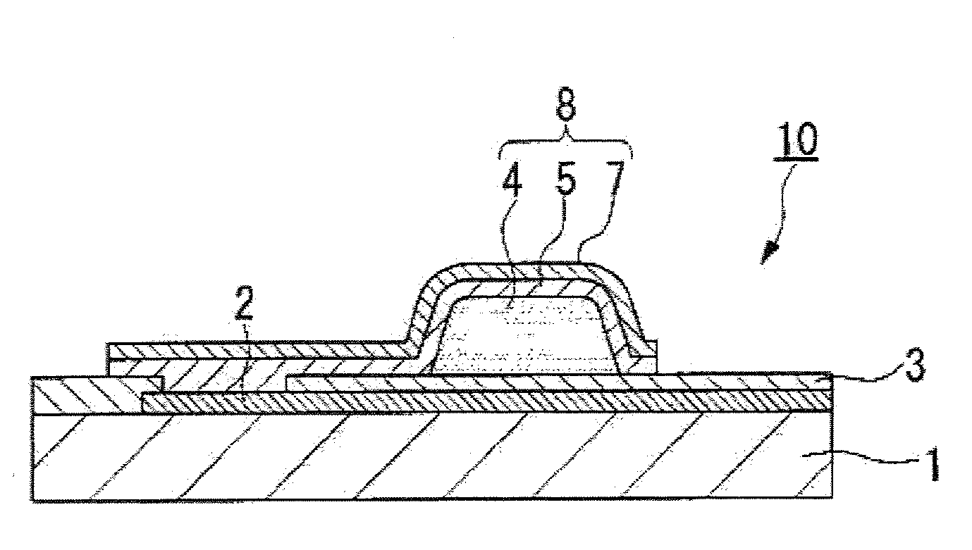
[0047]Semiconductor Device

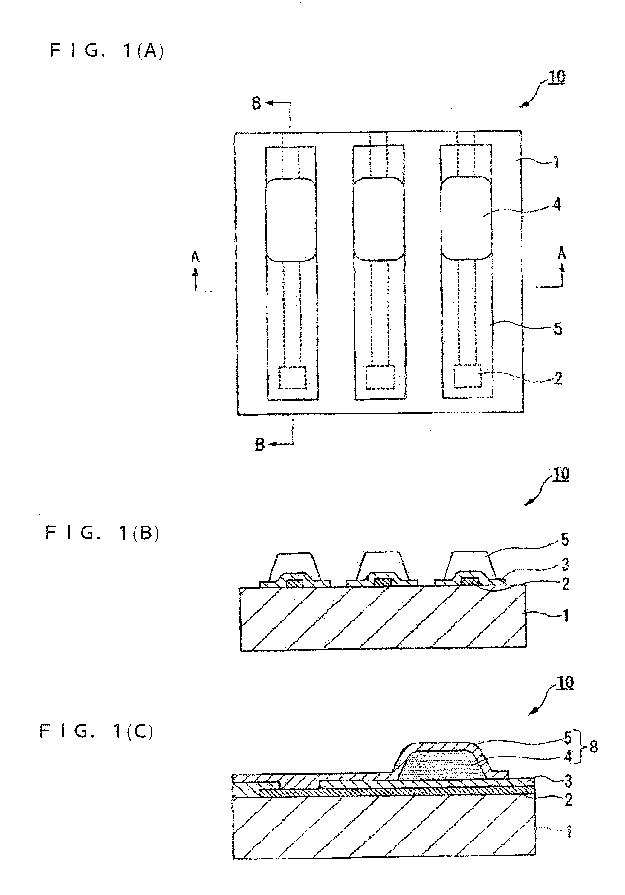
[0048]FIG. 1A is a partial enlarged top view of a substrate on which a semiconductor element is formed, showing a semiconductor device according to the present invention. FIG. 1B is a cross-sectional view along line A-A in FIG. 1A. FIG. 1C is another cross-sectional view along line B-B in FIG. 1A. In addition, the substrate in the present embodiment can be either a semiconductor substrate such as a silicon wafer on which a number of semiconductor chips are formed or an independent semiconductor chip. Further, in the case of a semiconductor chip, the shape of the chip is not limited to a general rectangular parallelpiped (i...

second embodiment

[0065]The second embodiment will now be described in detail referring to the accompanying drawings.

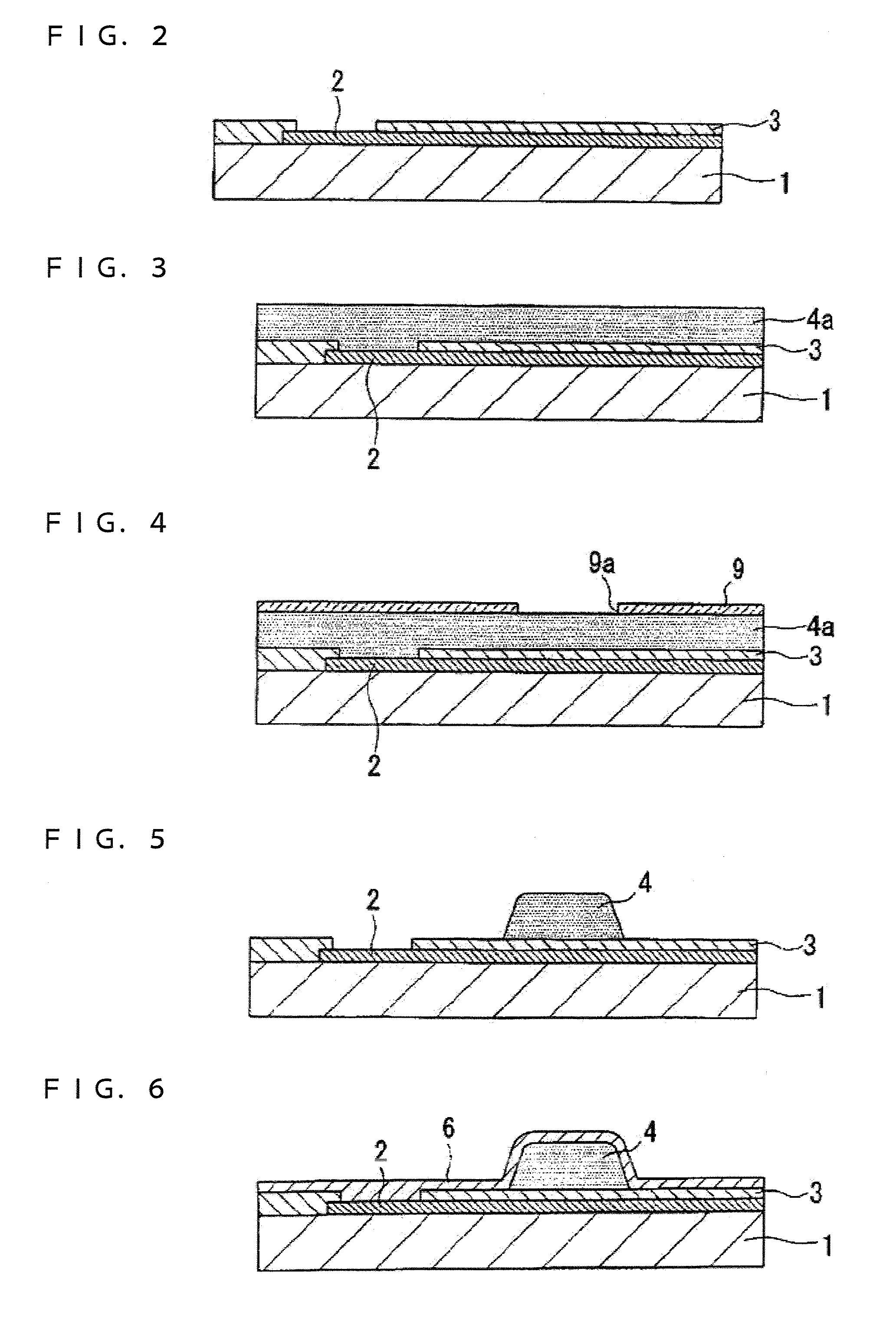
[0066]In the method for forming a semiconductor device according to the first embodiment, the conductive unit covering from the electrode 2 and spreading over the surface of the protrusion 4 is formed with a single layer of the first conductive layer 5. In contrast, the second embodiment provides a different method wherein the conductive unit covering from the electrode 2 and spreading over the surface of the protrusion 4 is formed with two layers including the first conductive layer 5 and the second conductive layer 7. In addition, the other details of the method for forming a semiconductor device are the same as those of the first embodiment. Therefore, the same reference numerals are used for the components common to both embodiments and detailed description is omitted.

[0067]First, employing the manufacturing steps shown in FIGS. 2 to 6 of the first embodiment, an electrode 2, a res...


PUM

PropertyMeasurementUnit
glass transition temperatureaaaaaaaaaa
temperatureaaaaaaaaaa

Abstract

A method of forming a bonded structure comprises the steps of: mounting a semiconductor device having an electrode; a convexity protruding higher than the electrode and formed of a resin; and a conductive unit electrically coupled to the electrode and extending over the surface of the convexity, onto a specific substrate with an intermediary of a bonding material; and mounting the semiconductor device by hot pressing within a temperature range including the glass transition temperature of the resin.

Description

RELATED APPLICATIONS[0001]This application is a continuation of U.S. patent application Ser. No. 11 / 103,942 filed Apr. 12, 2005. This application claims the benefit of Japanese Patent Application No. 2004-130866 filed Apr. 27, 2004 and 2005-008686 filed Jan. 17, 2005 which are hereby expressly incorporated by reference herein in their entirety.BACKGROUND[0002]1. Technical Field[0003]The present invention relates to a method of forming a bonded structure, as well as a circuit board, an electro-optic device and an electronic device.[0004]2. Related Art[0005]One conventional coupling method for bonding a driver IC on a substrate of a display device is a known as chip-on-glass (COG) coupling. The COG coupling employs a method wherein, for example, a driver IC is bonded by forming an Au-plated bump on a driver IC and then electrically coupling the bump formed on the driver IC with an electrode terminal formed on a substrate of a display device using a conductive bonding material such as ...

Claims


Application Information

Patent Timeline
Patent Type & Authority Applications(United States)
IPC IPC(8): B32B37/12B32B37/00H01L21/60G09F9/00H01L21/603H01L23/485
CPCH01L24/11H01L24/81H01L2224/0231H01L2224/114H01L2224/1147H01L2224/116H01L2224/13099H01L2224/16H01L2224/81801H01L2224/83191H01L2224/83192H01L2224/83193H01L2924/01013H01L2924/01022H01L2924/01029H01L2924/01046H01L2924/01074H01L2924/01078H01L2924/01079H01L2924/01082H01L2924/04941H01L2924/19041H01L2924/19043H01L2924/3025H01L24/13H01L2924/01005H01L2924/01006H01L2924/01024H01L2924/01033H01L2924/0105H01L2924/014H01L2224/13666H01L2224/13144H01L2224/13147H01L2224/13171H01L2224/1319H01L2224/13644H01L2224/13647H01L2224/13655H01L2224/13664H01L2224/13671H01L2224/13684H01L2224/13624H01L2924/0001H01L2224/0401Y10T156/10H01L2924/0665H01L2924/00014H01L2924/15788H01L2924/181H01L2224/05171H01L2224/05624H01L2224/05124H01L2224/05671H01L2224/05647H01L2224/05684H01L2224/05166H01L2224/05147H01L2224/05664H01L2224/05655H01L2224/05644H01L2224/05155H01L2224/05666H01L2224/051H01L2224/05164H01L2224/05144H01L2224/05184H01L2224/056H01L2224/13008H01L2224/13566H01L24/02H01L2924/00H01L2224/02H01L2924/013H01L2924/01023H01L21/52H01L23/12H01L23/48
Inventor TANAKA, SHUICHI
Owner SEIKO EPSON CORP
Why Eureka
Try Eureka