Display device and manufacturing method of display device

a technology of display device and manufacturing method, which is applied in the field of display device, can solve the problems of difficult to obtain sufficient characteristics, a number of processes for processing, and damage to organic semiconductor materials

Inactive Publication Date: 2009-10-15
RICOH KK
View PDF4 Cites 13 Cited by
  • Summary
  • Abstract
  • Description
  • Claims
  • Application Information

AI Technical Summary

Benefits of technology

[0015]In one aspect of the invention, the present disclosure provides an improved display device in which the above-described problems are eliminated.
[0016]In one aspect of the invention, the present disclosure provides a display device which is able to be manufactured with good quality and low cost, without adversely affecting the semiconductor material and the semiconductor chip, and raise the productivity.

Problems solved by technology

However, such vacuum processes require a number of processes.
The use of the plasma process may damage the organic semiconductor material, and it is difficult to obtain sufficient characteristics.
The use of the RIE may damage the organic semiconductor material, and it is difficult to obtain predetermined characteristics.
Specifically, when a wet-type spreading of an insulating material solved in an organic solvent is performed and a semiconductor material for forming the semiconductor chip is easily eroded by the organic solvent, the semiconductor material will be adversely influenced by the organic solvent.
It is difficult to obtain sufficient characteristics of the semiconductor chip formed by the semiconductor material.
When a semiconductor material for forming the semiconductor chip is vulnerable to heating, the semiconductor chip will be adversely influenced by heating.
It is difficult to obtain sufficient characteristics of the semiconductor chip.
For this reason, it takes much time to perform a manufacturing process including a series of processes, and the productivity will be reduced.
When the process of forming the display part includes a step of heating or UV irradiation and the semiconductor material which is easily damaged by heating or UV irradiation must be used, it is difficult to obtain sufficient characteristics of the semiconductor chip formed by the semiconductor material.
The interlayer insulation film which is adversely influenced by the supporting semiconductor layer may have surface irregularities.
If the electrodes are formed on the surface irregularities of the interlayer insulation film, occurrence of a disconnection or formation of a high resistance region may take place, which causes a defective semiconductor chip to be produced.
However, even if the CMP method is performed to make the surface of the interlayer insulation film flat, there is a possibility that the semiconductor layer be damaged by the CMP method.
In the case of the method disclosed in Japanese Laid-Open Patent Application No. 2007-103484, the semiconductor material may be adversely influenced by the organic solvent used to mix the organic material with the fine particles, which will affect the characteristics of the semiconductor chip.

Method used


Image

  • Display device and manufacturing method of display device
  • Display device and manufacturing method of display device
  • Display device and manufacturing method of display device

Examples


first embodiment

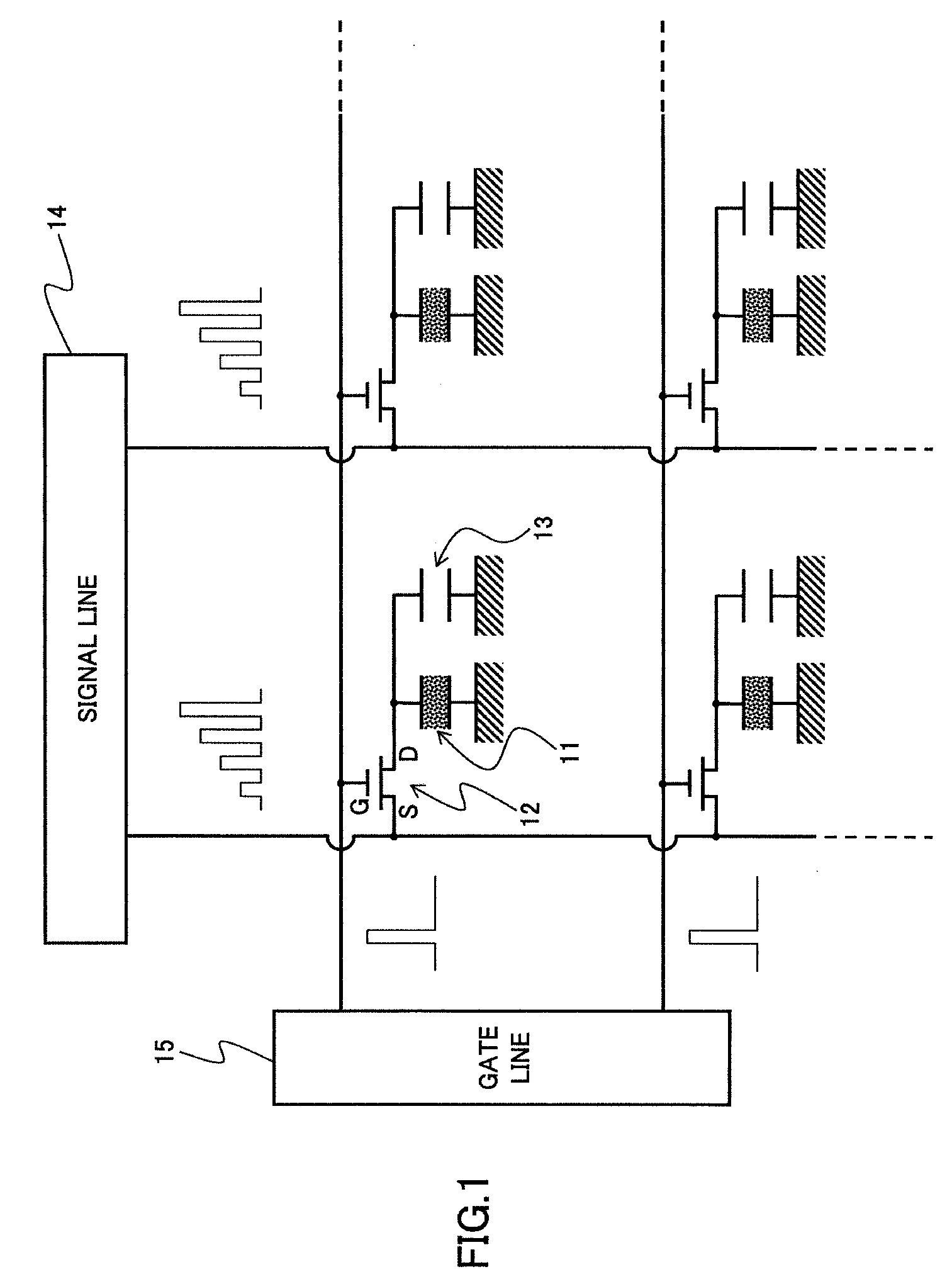
[0042]the invention will be described. This embodiment relates to a method of manufacturing an electrophoretic display device. FIG. 1 shows the composition of a drive circuit of the electrophoretic display device of this embodiment.

[0043]Specifically, as shown in FIG. 1, a FET (field effect transistor) 12 and a pixel capacitor 13 are arranged for every pixel of the display device to drive an image displaying element 11 which is an electrophoretic display element used as one pixel.

[0044]In the FET 12, the gate (G) is connected to a gate line 15, the source (S) is connected to a signal line 14, and the drain (D) is connected to both one electrode of the image displaying element 11 and one electrode of the pixel capacitor 13. Both the other electrode of the image displaying element 11 and the other electrode of the pixel capacitor 13 are grounded.

[0045]In the drive circuit, the voltage supplied from the signal line 14 according to the gray scale of each pixel, and the gate voltage from...

second embodiment

[0084]Next, the invention will be described. This embodiment relates to a method of manufacturing an electrophoretic display device. The composition of a drive circuit for driving the electrophoretic display device of this embodiment is shown in FIG. 7.

[0085]Specifically, as shown in FIG. 7, the drive circuit of this embodiment is a drive circuit which supplies current to a current drive type display element to drive the display element. To drive the display element 111 which is an electrophoretic display element used as one pixel, two FETs (field effect transistors) 112 and 113, and a pixel capacitor 114 are formed for every pixel.

[0086]In the FET 112, the gate (G) is connected to the gate line 115, the source (S) is connected to the signal line 117, and the drain (D) is connected to both the gate (G) of the FET 113 and the electrode of the pixel capacitor 114. The electrode of another side of the pixel capacitor 114 is connected to the capacitor line 116.

[0087]In the FET 113, the ...

fourth embodiment

[0159]Next, the invention will be described.

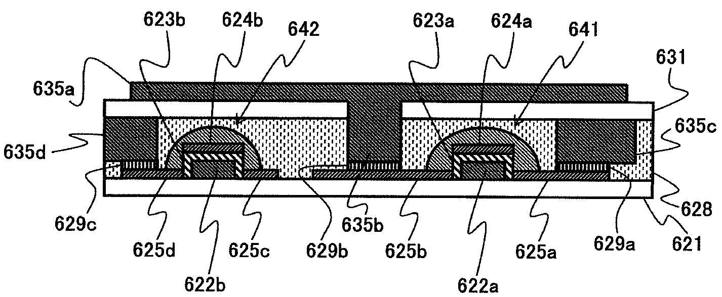
[0160]The fourth embodiment is formation method with another electrode of the second substrate 31 and 131 about the first embodiment and second embodiment, and explains the case where an electrode is formed in what serves as the second substrate 131 of the second embodiment concretely.

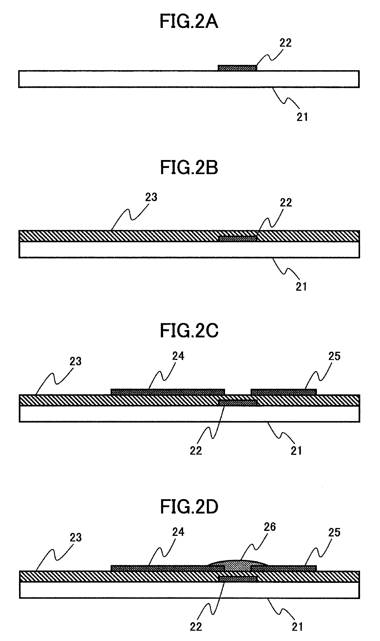
[0161]First, as shown in FIG. 17A, contact hole 332 is formed in the second substrate 331. The formation method is the same as that of the first embodiment and the second embodiment.

[0162]Next, as shown in FIG. 17B, resist pattern 333 is formed in the region in which the electrode of both sides of the second substrate 331 is not formed. After applying resist to both sides of the second substrate 331, specifically, resist pattern 333 is formed by performing prebaking, exposure by the exposing device, and development.

[0163]As for this resist pattern, it is desirable to form more thickly than the thickness of the electrode formed behind. It is possible to form t...


PUM

PropertyMeasurementUnit
anisotropicaaaaaaaaaa
anisotropic conductionaaaaaaaaaa
semiconductoraaaaaaaaaa

Abstract

A display device includes a first substrate on which a semiconductor circuit is formed. A second substrate is disposed over the first substrate to include a first electrode formed on a first surface to perform image displaying, and a second electrode exposed to a second surface and bonded to the first electrode via a contact hole. A third substrate is disposed over the second substrate to include a third electrode formed to perform image displaying in association with the first electrode of the second substrate. An image displaying layer is disposed between the second substrate and the third substrate to perform image displaying. An electrode on a surface of the first substrate on which the semiconductor circuit is formed is electrically connected to the second electrode exposed to the second surface of the second substrate.

Description

BACKGROUND OF THE INVENTION[0001]1. Field of the Invention[0002]This invention relates to a display device which can be manufactured with a low cost, and a manufacturing method of a display device which can manufacture a display device with a low cost.[0003]2. Description of the Related Art[0004]Conventionally, when producing a display element for use in a display device, a semiconductor fabrication process is used to form a semiconductor circuit for driving the display element, on a substrate, such as a glass substrate, and form an insulating layer on the semiconductor circuit, and further form the display element on the insulating layer. Namely, the semiconductor circuit for driving the display element and the display element are formed one by one by laminating such films on the glass substrate.[0005]For this reason, as disclosed in Japanese Laid-Open Patent Application No. 2004-104134, it is necessary to form a thick interlayer insulation film after the semiconductor circuit is f...

Claims


Application Information

Patent Timeline
Patent Type & Authority Applications(United States)
IPC IPC(8): H01L33/00G02F1/1343G02F1/1368G09F9/00G09F9/30H01L51/50H05B33/10H05B33/14H05B33/26
CPCG02F2201/42G02F1/1345
Inventor KONDO, HIROSHIYASHIRO, TOHRUNAKAMURA, YUKISHIBUYA, TAKESHIHIRANO, SHIGENOBUABE, YUKIKO
Owner RICOH KK
Why Eureka
Try Eureka