Top Gate Thin Film Transistor with Independent Field Control for Off-Current Suppression

a thin film transistor and field control technology, applied in the field of integrated circuit (ic) fabrication, can solve the problems of higher off-current levels and inoptimal structures, and achieve the effects of low contact resistance, reduced manufacturing cost, and reduced manufacturing costs

Active Publication Date: 2009-10-15
SHARP KK
View PDF13 Cites 12 Cited by
  • Summary
  • Abstract
  • Description
  • Claims
  • Application Information

AI Technical Summary

Benefits of technology

[0009]Conventional bottom-gate TFT and top-gate structure are simple to fabricate using well-established process flows. These structures may be optimal for an a-Si active layer because the gate/contact overlap ensures low contact resistance without causing a high off-current. However, these structures are not necessarily optimal when a mid-mobility active layer such as μc-Si is used. When μc-Si replac

Problems solved by technology

However, these structures are not necessarily optimal when a mid-mobility active layer such as μc-Si is used.
The sm

Method used


Image

  • Top Gate Thin Film Transistor with Independent Field Control for Off-Current Suppression
  • Top Gate Thin Film Transistor with Independent Field Control for Off-Current Suppression
  • Top Gate Thin Film Transistor with Independent Field Control for Off-Current Suppression

Examples


Embodiment Construction

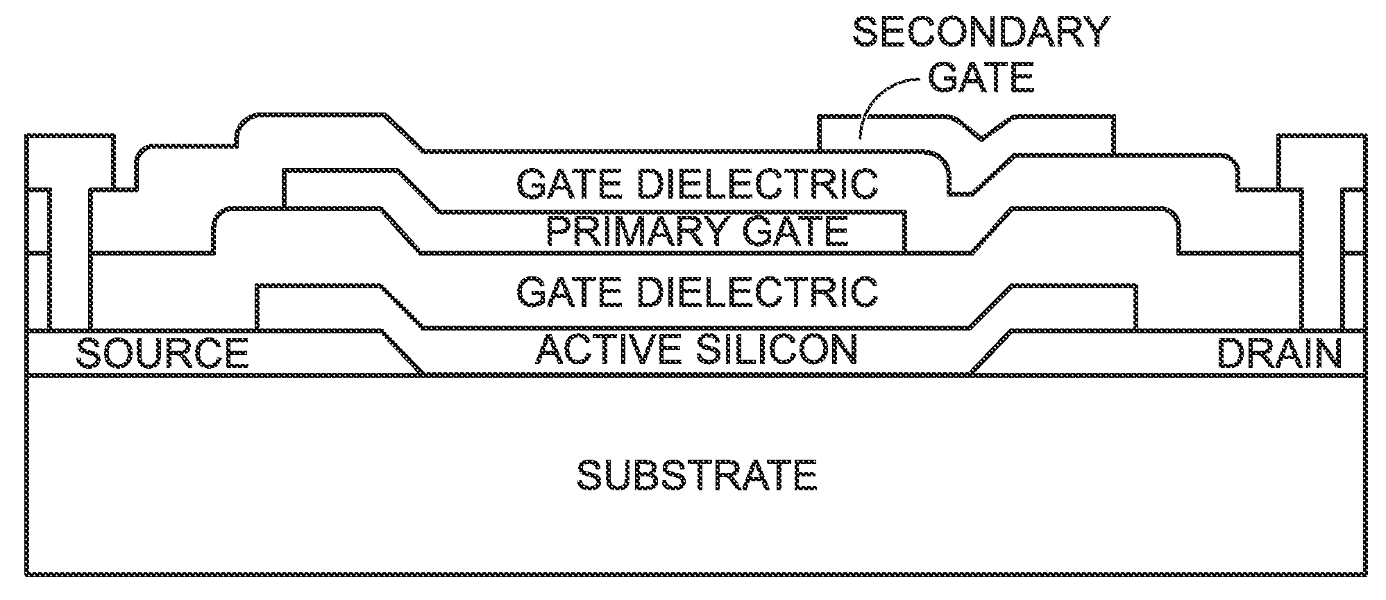
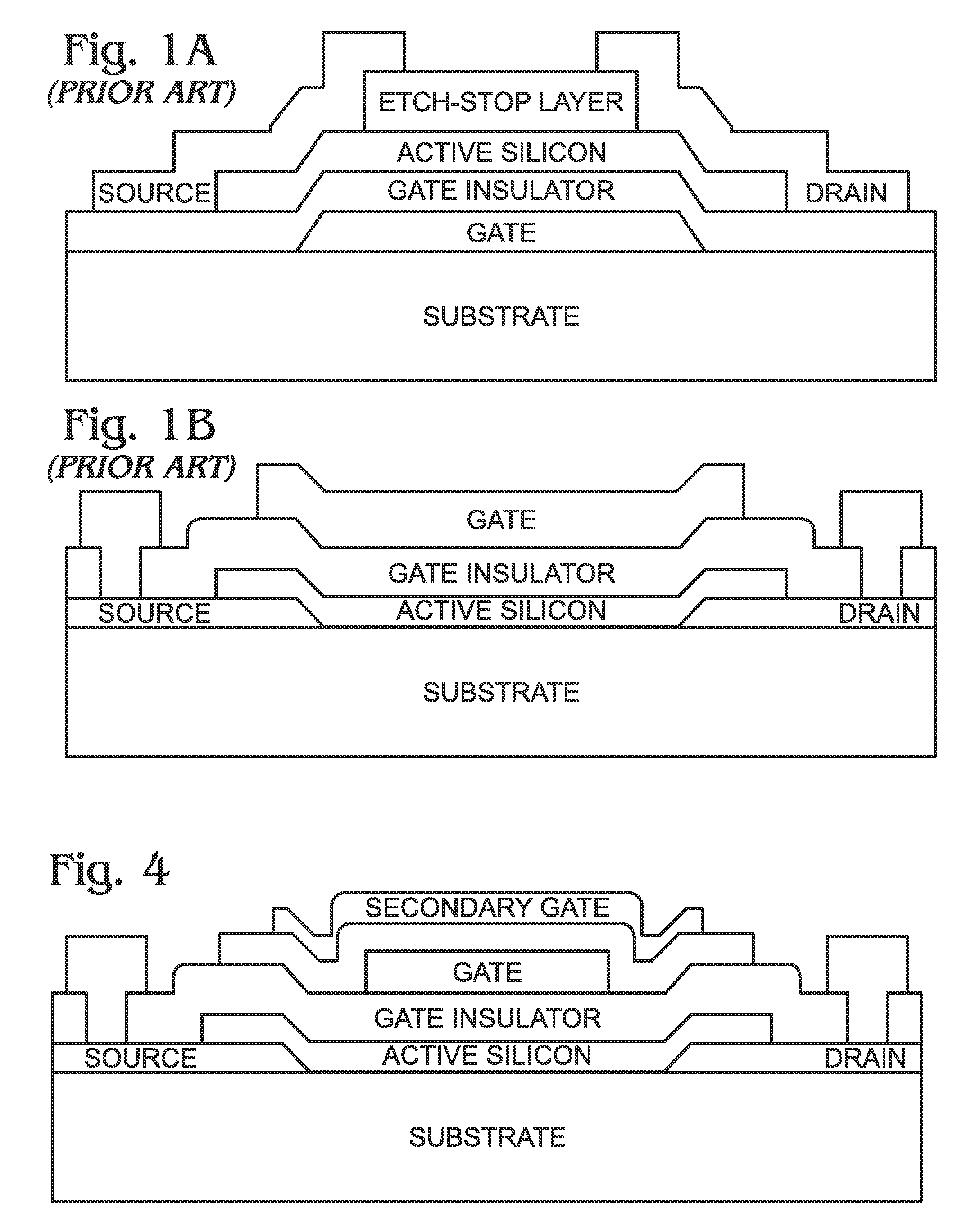
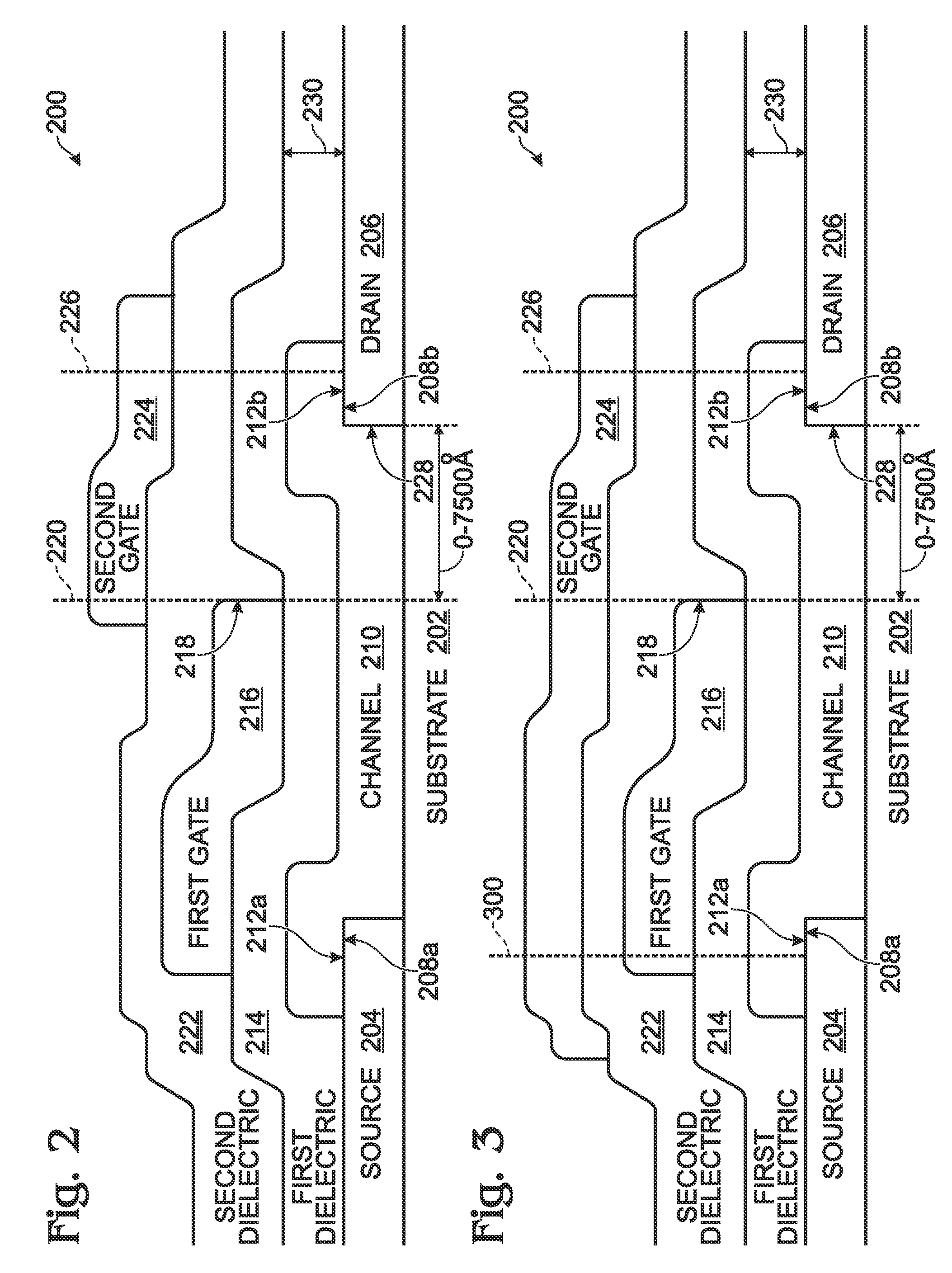
[0022]FIG. 2 is a partial cross-sectional view of a bottom-contacted top gate (TG) thin film transistor (TFT) with independent field control for off-current suppression. The TFT 200 comprises a substrate 202, which may be a material such as metal foil, Si, glass, plastic, or quartz. However, other unnamed substrate materials may also be used that are well known in the art. A source region 204 and a drain region 206 overlie the substrate 202, each having a channel interface top surface 208a and 208b, respectively. A channel 210 is interposed between the source 204 and drain 206, with a source contact regions 212a and a drain contact 212b immediately overlying the source / drain (S / D) interface top surfaces 208a and 208b, respectively.

[0023]In one aspect, the source 204 and drain 206 regions are a first material, and the channel 210 is a second material different than the first material. For example, the source 204 and drain 206 regions may be materials such as a-Si, microcrystalline Si...


PUM


Abstract

A bottom-contacted top gate (TG) thin film transistor (TFT) with independent field control for off-current suppression is provided, along with an associated fabrication method. The method provides a substrate, and forms source and drain regions overlying the substrate, each having a channel interface top surface. A channel is interposed between the source and drain, with source and drain contact regions immediately overlying the source/drain (S/D) interface top surfaces, respectively. A first dielectric layer is formed overlying the source, drain, and channel. A first gate is formed overlying the first dielectric, having a drain sidewall located between the contact regions. A second dielectric layer is formed overlying the first gate and first dielectric. A second gate overlies the second dielectric, located over the drain contact region.

Description

BACKGROUND OF THE INVENTION[0001]1. Field of the Invention[0002]This invention generally relates to integrated circuit (IC) fabrication and, more particularly, to a two-gate structure that permits enhanced off-current suppression in a top gate thin-film transistor (TFT).[0003]2. Description of the Related Art[0004]FIGS. 1A and 1B are, respectively, partial cross-sectional views of bottom gate and top gate TFT devices made using an amorphous silicon (Si) active layer (prior art). For ease of fabrication using well-established process flows, the channel is formed from a thin-film material that is interposed between the source and drain, while overlapping the regions (contact regions) of the source and drain. Such a structure is optimal for an amorphous Si (a-Si) active layer because the gate / contact overlap ensures low contact resistance without causing high off-current.[0005]To economically fabricate higher quality consumer devices such a liquid crystal display (LCD) televisions, so-...

Claims


Application Information

Patent Timeline
IPC IPC(8): H01L27/12H01L21/00H01L29/786
CPCH01L29/42384H01L29/78696H01L29/78645H01L29/78609
Inventor KISDARJONO, HIDAYATVOUTSAS, APOSTOLOS T.
Owner SHARP KK
Why Eureka
Try Eureka