

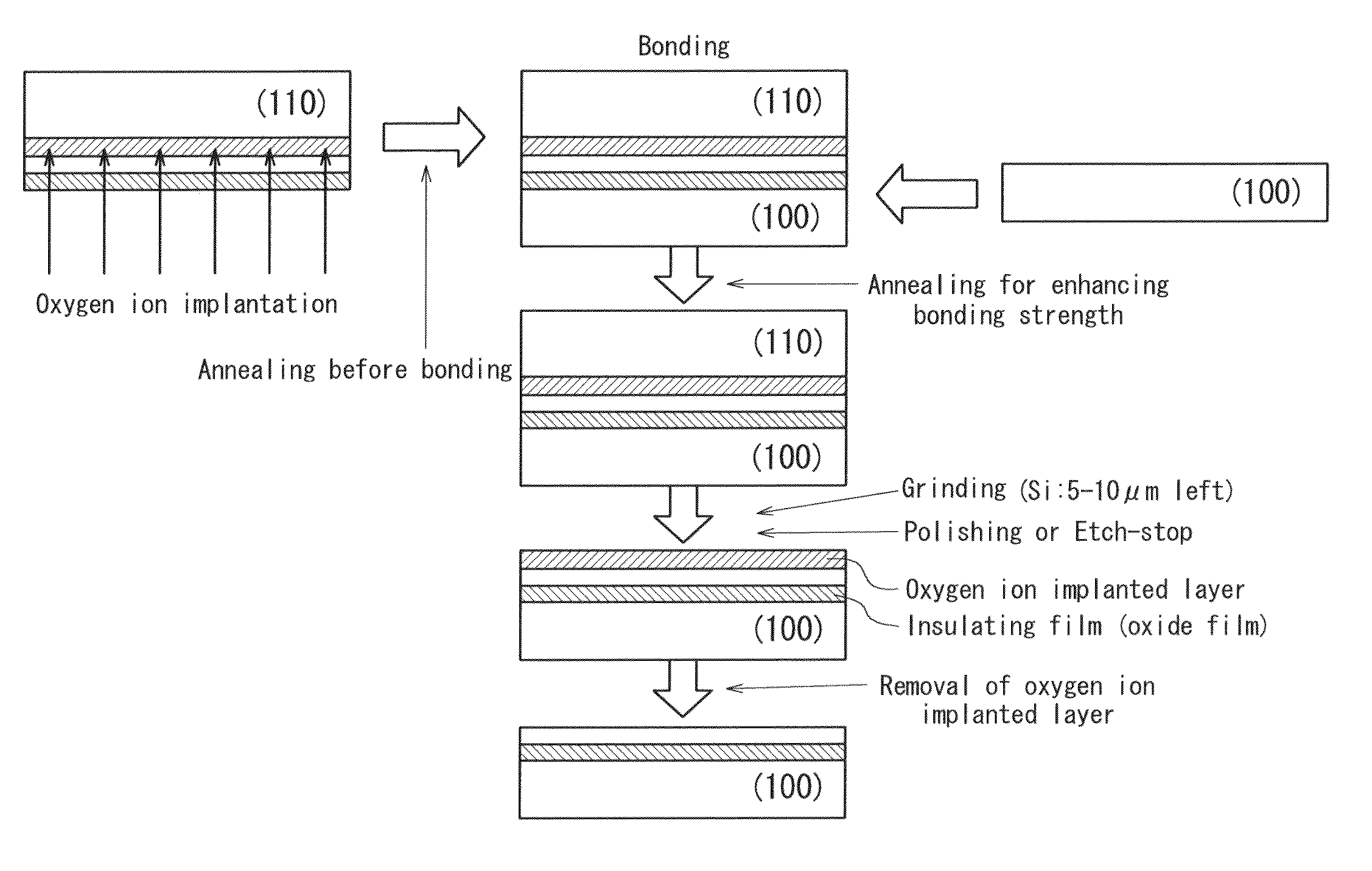
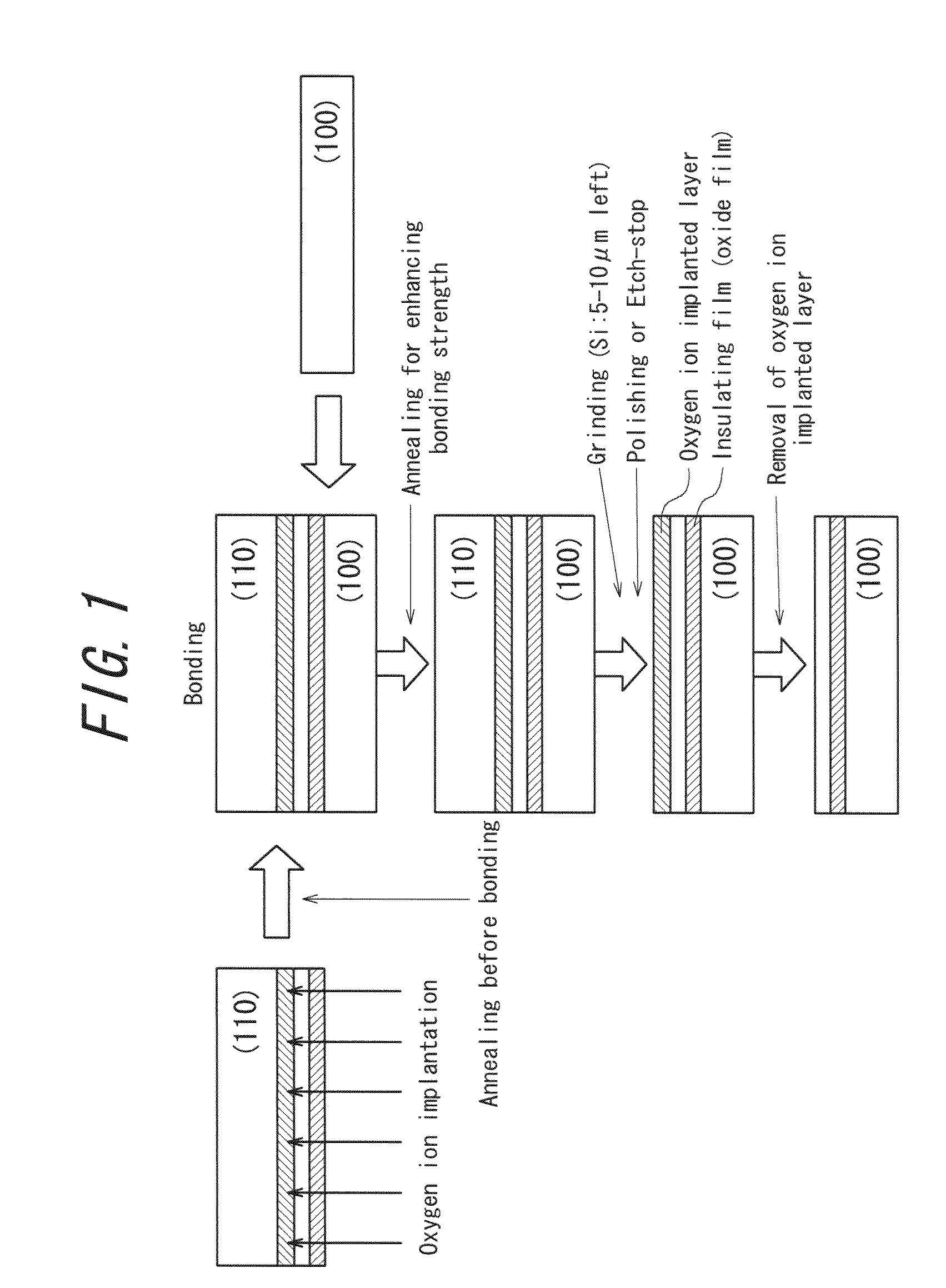
Method for producing bonded wafer
a technology of bonded wafers and bonded layers, which is applied in the manufacture of basic electric elements, semiconductor/solid-state devices, electrical equipment, etc., can solve the problems of its fabrication accuracy and the risk of thinning of oxygen ion implanted layers, and achieve the effect of effectively removing them
- Summary
- Abstract
- Description
- Claims
- Application Information
AI Technical Summary
Benefits of technology
Problems solved by technology
Method used
Image

Examples
example 1
[0111]There are provided two silicon wafers of 300 mm in diameter sliced from a silicon ingot grown by CZ method and doped with boron. Both of the two wafers have a crystal orientation of (100) and are p-type having a specific resistance of 1 to 10 Ωcm. One of the two silicon wafers is used as a wafer for active layer, and this (100) wafer is treated in an oxidizing atmosphere at 1000° C. for 5 hours to form an oxide film having a thickness of 150 nm.
[0112]Then, an oxygen ion implantation is carried out from the surface of the (100) wafer in two stages at an acceleration voltage of 200 keV. The first oxygen ion implantation is conducted under conditions of substrate temperature: 200 to 600° C. and doset: 1×10¹⁶ to 5×10¹⁷ atoms / cm2. The second oxygen ion implantation is conducted under conditions of substrate temperature: room temperature to 300° C. and dose: 1×10¹⁵ to 1×10⁶ atoms / cm2. As a result, an oxygen ion implanted layer is formed at a depth position of about 400 nm from the s...
PUM
 Abstract
Description
Claims
Application Information