Bandwidth reduction mechanism for polar modulation

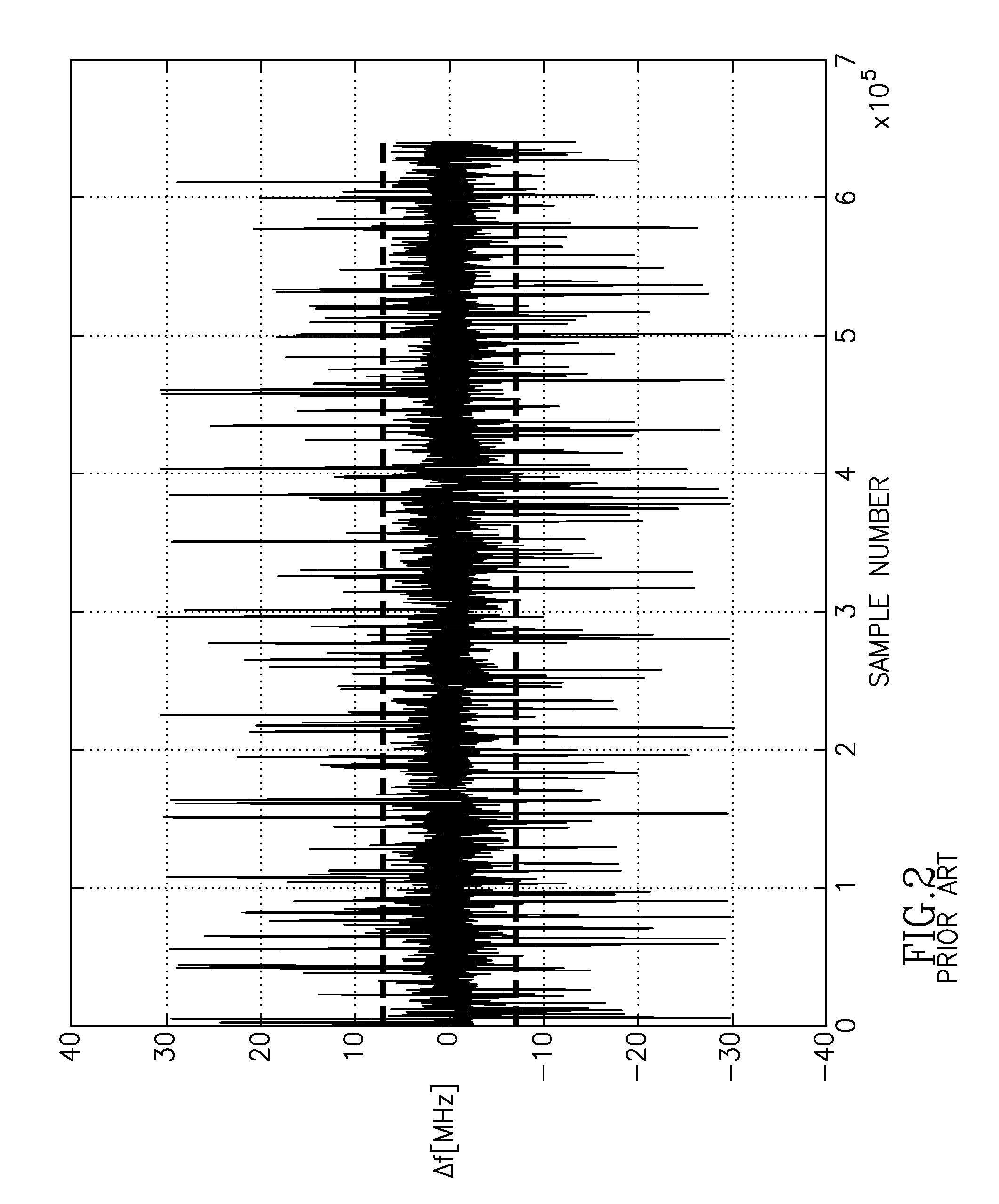
a polar modulation and bandwidth reduction technology, applied in the field of data communication, can solve the problems of inability to meet the fabrication cost of rf/analog circuit mask adders, the implementation of traditional rf circuits is complicated, and the bandwidth is too large for a single oscillator (i.e. the dco) to handle, so as to reduce the modulation bandwidth, and reduce the polar modulation bandwidth

Active Publication Date: 2009-10-15
TEXAS INSTR INC
View PDF11 Cites 48 Cited by
  • Summary
  • Abstract
  • Description
  • Claims
  • Application Information

AI Technical Summary

Benefits of technology

[0036]There is also provided in accordance with the invention, a method of reducing polar modulation bandwidth, the method comprising the steps of receiving TX IQ data samples, converting the TX IQ data samples into amplitude samples and phase / frequency samples, detecting a distance to an origin of complex domain trajectory of the amplitude samples and phase / frequency samples and modifying the complex domain trajectory if the distance to the origin is less than a predetermined threshold distance.
[0037]There is further provided in accordance with the invention, an apparatus for reducing polar modulation bandwidth comprising a zero crossing detector operative to determine a complex domain trajectory of input TX IQ data samples and to detect the passing of the complex domain trajectory within a predetermined threshold distance from an origin and a path modification circuit operative to modify the complex domain trajectory in response to the detection so as to reduce the modulation bandwidth thereby.
[0038]There is also provided in accordance with the invention, an apparatus for reducing the bandwidth of a polar modulator comprising a filter for generating trajectory sample points, a zero crossing detector operative to determine a complex domain trajectory of input TX IQ data samples and to detect the passing of the complex domain trajectory within a predetermined threshold distance from an origin and an offset vector generator operative to generate an offset vector which, when added to the TX IQ data samples, maintains the complex domain trajectory beyond the predetermined threshold distance from the origin thereby reducing the polar modulation bandwidth.
[0039]There is further provided in accordance with the invention, a polar radio frequency (RF) transmitter comprising a bandwidth reduction circuit comprising a filter for generating trajectory sample points, a zero crossing detector operative to determine a complex domain trajectory of input TX IQ data samples and to detect the passing of the complex domain trajectory within a predetermined threshold distance from an origin, an offset vector generator operative to generate an offset vector which, when added to the TX IQ data samples, maintains the complex domain trajectory beyond the predetermined threshold distance from the origin thereby reducing the polar modulation bandwidth, a combiner for adding the offset vector to the TX IQ data samples to generate modified TX IQ data samples thereby, means for generating a frequency command and an amplitude command in accordance with the modified TX IQ data samples, a frequency synthesizer operative to generate an RF signal having a frequency in accordance with a frequency reference input and the frequency command and a digital power amplifier (DPA) operative to receive the RF signal and to generate a modulated RF output signal in proportion to the amplitude command.

Problems solved by technology

The use of low-voltage deep submicron CMOS processes allows for an unprecedented degree of scaling and integration in digital circuitry, but complicates implementation of traditional RF circuits.
Furthermore, any mask adders for RF / analog circuits are not acceptable from a fabrication cost standpoint.
This bandwidth, however, might be too large for a single oscillator (i.e. the DCO) to handle while still providing the needed granularity (i.e. quantization step size, phase noise, etc.) and frequency coverage to span all frequency bands, including the typical bands of GSM-EU, GSM-US, PCS, DCS and IMT2K.
Since the DCO modulation range is limited, frequency data is truncated resulting in a severely degraded error vector magnitude (EVM).
A disadvantage of this solution is that since the DCO circuit incorporates a large monolithic inductor, significant area would be consumed.
Even if such a solution was constructed, it is not certain whether (1) the full modulation range (i.e. fine frequency step) could be achieved while keeping the DCO phase noise within specification or (2) whether the EVM would be degraded and compromised.
Such a high (possibly infinite) phase bandwidth makes it difficult and impractical to implement a polar modulator because it requires a very fast change of the oscillator phase (i.e. very wide frequency modulation of the oscillator).
This is disadvantageous when, during the complex modulation, the I / Q vector is close to the origin (i.e. small amplitude) and makes fast, large phase / frequency changes, such as indicated by the example trajectories in FIG. 5 as it passes near and through the origin, versus small phase / frequency changes which occur relatively far from the origin.
A polar architecture that may be suitable for EDGE transmission may not be readily used for certain modulation schemes such as those used in WCDMA and WLAN transmission because the modulation data rate is very high in these schemes with the resultant difficulty of performing high frequency modulation of the DCO and the amplitude.
Digital I / Q modulation, on the other hand, has the same disadvantages of the amplitude modulation part of polar transmission, and has I and Q summed together without the benefits of the fine frequency resolution of the polar modulator.
Additionally, the phase and amplitude mismatch of the I and Q paths can result in a severe distortion of the modulated signal when the two paths are finally recombined.
The advantages of frequency modulation, namely a very fine step size of frequency control, however, becomes a disadvantage in cases where large frequency deviations are required to be performed (see FIG. 2).
Note that with digital I / Q modulation, the I and Q quadrature components are regulated digitally in an open loop system and thus typically suffer dynamic-range / accuracy limitations.
This limits the accuracy in the phase domain compared to what is achievable in a polar structure where a closed loop system is used to achieve very fine frequency resolution.
A limitation with using an analog quad-switch at the output of the DCO to achieve fast phase modulation is that the analog quad-switch can only achieve + / −90 to + / −180 degree phase jumps.
Thus, any residue phase must be compensated with the DCO frequency modulation, which suffers from phase discontinuity and excessive phase noise.

Method used


Image

  • Bandwidth reduction mechanism for polar modulation
  • Bandwidth reduction mechanism for polar modulation
  • Bandwidth reduction mechanism for polar modulation

Examples


Embodiment Construction

Notation Used Throughout

[0069]The following notation is used throughout this document.

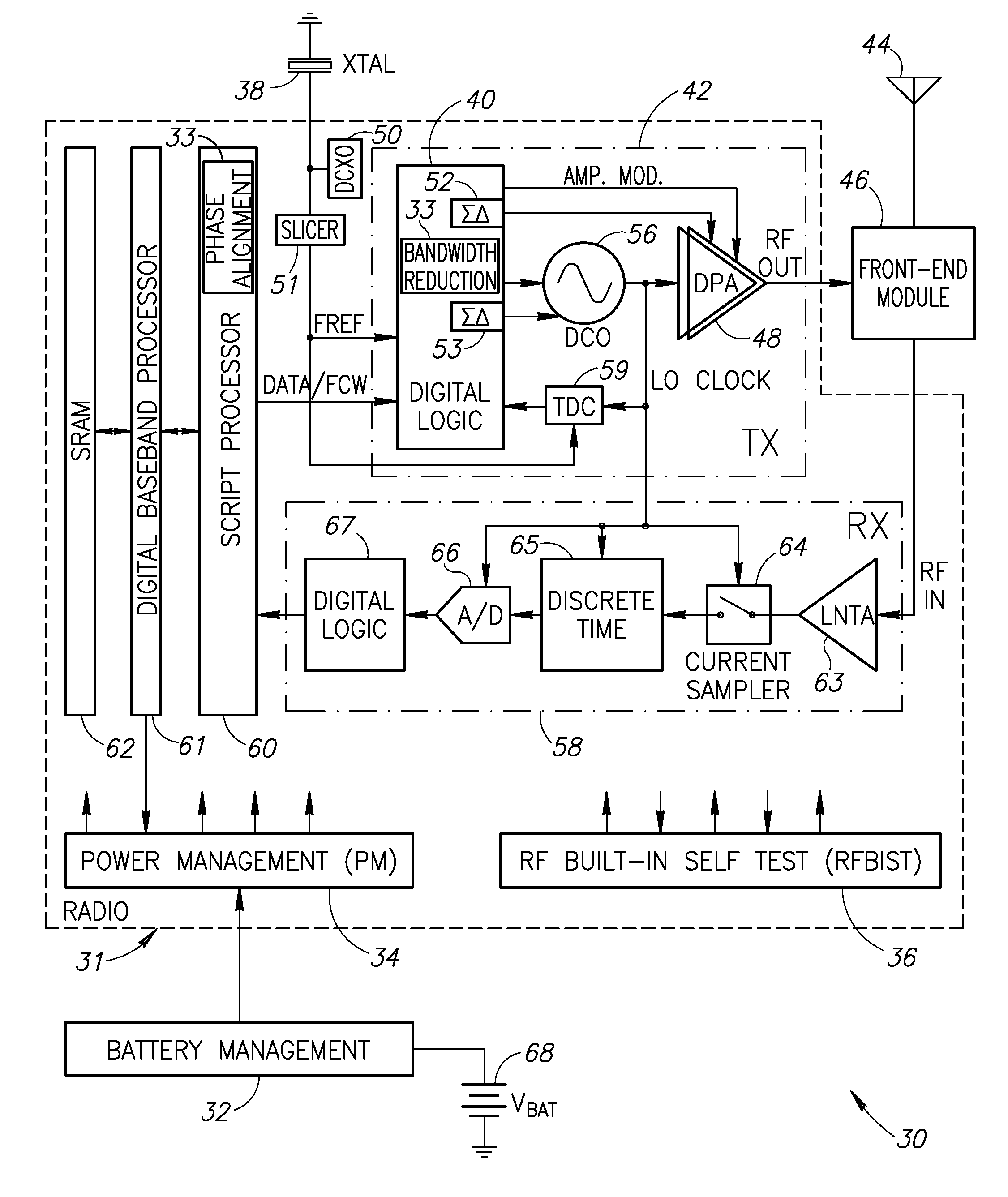
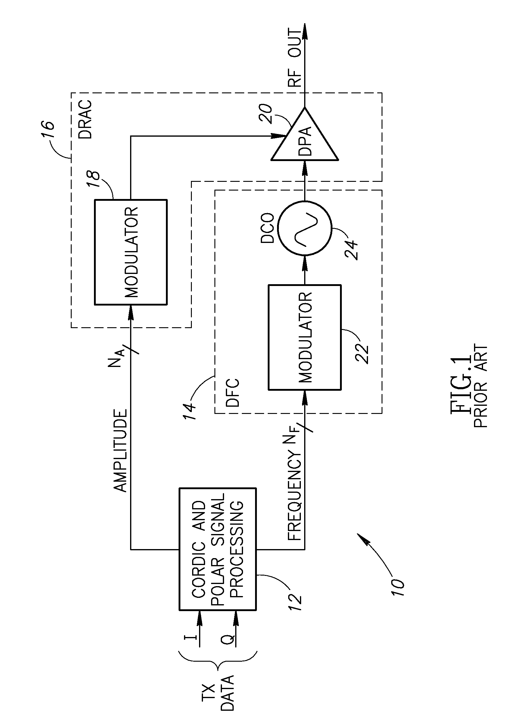
TermDefinitionACAlternating CurrentACWAmplitude Control WordADCAnalog to Digital ConverterADPLLAll Digital Phase Locked LoopAMAmplitude ModulationASICApplication Specific Integrated CircuitAVIAudio Video InterfaceBISTBuilt-In Self TestBMPWindows BitmapBWBandwidthBWRBandwidth ReductionCICCascaded Integrator-CombCMOSComplementary Metal Oxide SemiconductorCORDICCOordinate Rotation DIgital ComputerCPUCentral Processing UnitDACDigital to Analog ConverterdBDecibelDBBDigital BasebandDCDirect CurrentDCODigitally Controlled OscillatorDCSDigital Cellular SystemDCXODigitally Controlled Crystal OscillatorDFCDigital-to-Frequency ConversionDPADigitally Controlled Power AmplifierDPPADigital Pre-Power AmplifierDRACDigital to RF Amplitude ConversionDRPDigital RF Processor or Digital Radio ProcessorDSLDigital Subscriber LineDSPDigital Signal ProcessorEDGEEnhanced Data Rates for GSM EvolutionEEPROMElectrically Erasab...


PUM


Abstract

A novel and useful apparatus for and method of reducing phase and amplitude modulation bandwidth in polar transmitters. The bandwidth reduction mechanism of the present invention effectively reduces the phase modulation bandwidth of the polar modulation performed in the transmitter by modifying the zero-crossing trajectories in the IQ domain. This significantly reduces the phase modulation bandwidth while still meeting the output spectrum and error vector magnitude (EVM) requirements of the particular modern wideband wireless standard, such as 3G WCDMA, etc. The mechanism detects a zero crossing or a near zero crossing within a predetermined threshold of the origin and an offset vector is generated that when added to the input TX IQ data, shifts the trajectory to avoid the origin thus reducing the resultant polar modulation amplitude and phase bandwidth.

Description

REFERENCE TO PRIORITY APPLICATION[0001]This application claims priority to U.S. Provisional Application Ser. No. 61 / 043,432, filed Apr. 9, 2008, entitled “Bandwidth Reduction Technique for Polar Modulation,” incorporated herein by reference in its entirety.FIELD OF THE INVENTION[0002]The present invention relates to the field of data communications and more particularly relates to an apparatus for and method of reducing phase and amplitude modulation bandwidth in polar transmitters.BACKGROUND OF THE INVENTION[0003]With the explosive growth of the cellular phone industry, the need has arisen to reduce cost and power consumption of mobile handsets. To keep costs down, the entire radio, including memory, application processor, digital baseband processor, analog baseband and RF circuits, would ideally be all integrated onto a single silicon die with a minimal count of external components. The use of low-voltage deep submicron CMOS processes allows for an unprecedented degree of scaling ...

Claims


Application Information

Patent Timeline
Patent Type & Authority Applications(United States)
IPC IPC(8): H04B1/04
CPCH03C5/00
Inventor ZHUANG, JINGCHENGSTASZEWSKI, ROBERT B.WAHEED, KHURRAM
Owner TEXAS INSTR INC
Why Eureka
Try Eureka