

Boron nitride and boron-nitride derived materials deposition method
a boron nitride and derived material technology, applied in the direction of basic electric elements, electrical equipment, semiconductor devices, etc., can solve the problems of large thermal cycle of the gate device, material lack of structural integrity, and excessive signal crosstalk between adjacent interconnection lines
- Summary
- Abstract
- Description
- Claims
- Application Information
AI Technical Summary
Benefits of technology
Problems solved by technology
Method used
Image

Examples
Embodiment Construction
[0018]The present invention encompasses forming dielectric material adjacent substrate features, such as forming spacer materials for double patterning processes and for gate stacks by applying a boron-based material to the substrate structures. In one embodiment, a spacer material is formed by depositing and etching a boron nitride material, which material may optionally include hydrogen, carbon, oxygen, silicon, chlorine, and combinations thereof. In another embodiment, a spacer material may be formed by depositing a boron-nitride layer, depositing a liner layer on the boron-nitride layer, etching the liner layer, and etching the boron-nitride layer.
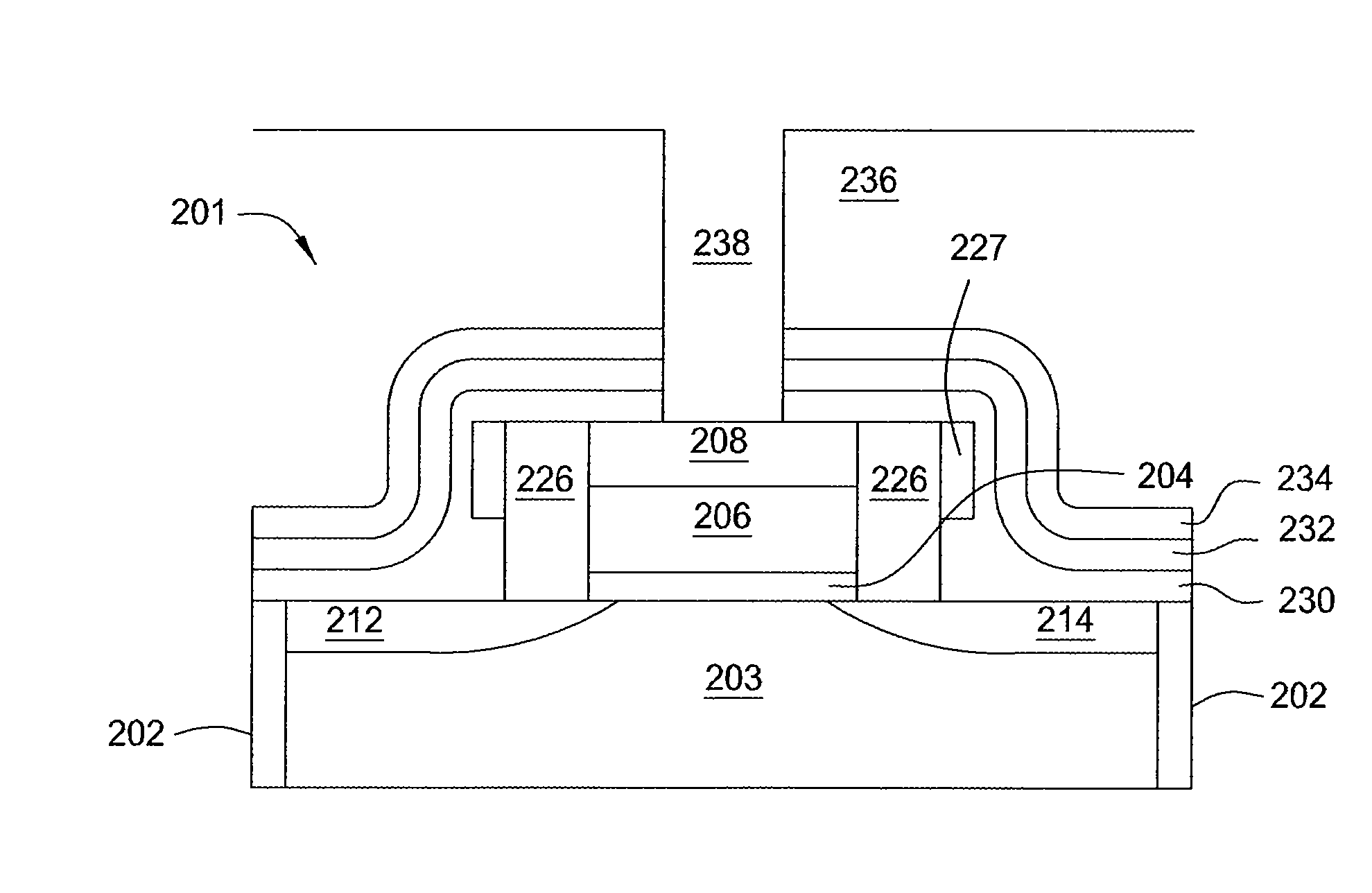
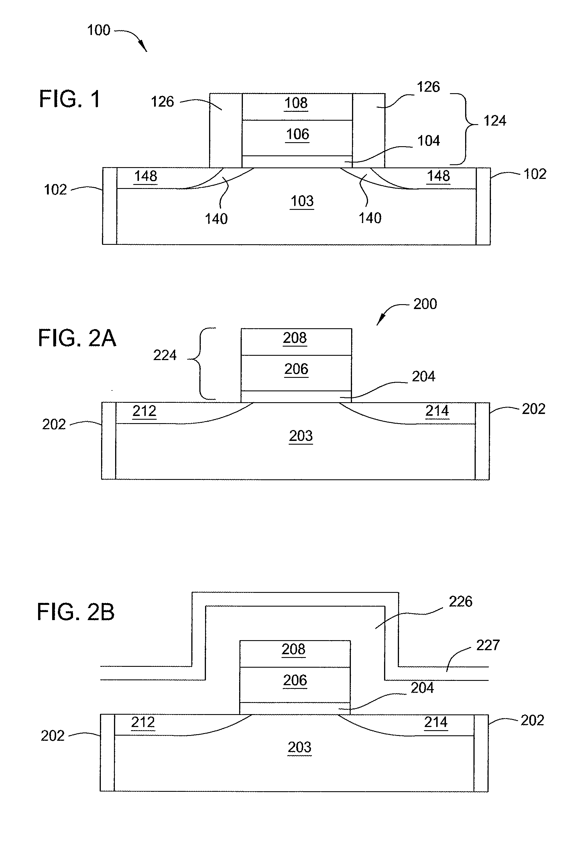
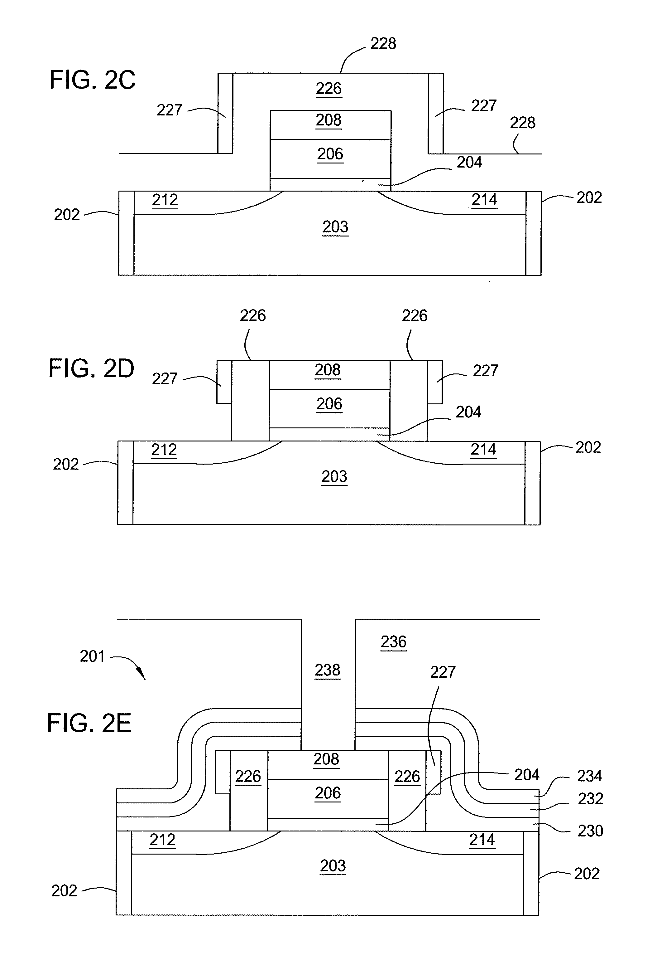
[0019]FIG. 1 illustrates a transistor having a gate structure formed according to one embodiment of the invention. Referring to FIG. 1, a plurality of field isolation regions 102 are formed in a substrate 100, for example, a silicon wafer. The plurality of field isolation regions 102 isolate a well region 103 of one type conductivity, ...
PUM
 Abstract
Description
Claims
Application Information