Photovoltaic wire

a photovoltaic wire and nano-structure technology, applied in the direction of photovoltaic energy generation, semiconductor devices, solid-state devices, etc., can solve the problems of more problematic charge separation and collection using nano-sized structures, and achieve the effects of improving light absorption, increasing absorption, and enhancing optical absorption of nanowires

Inactive Publication Date: 2009-10-29
ILLUMINEX CORP
View PDF24 Cites 51 Cited by
  • Summary
  • Abstract
  • Description
  • Claims
  • Application Information

AI Technical Summary

Benefits of technology

[0003]The present invention relates generally to a nanostructured photovoltaic device that can be formed as a ribbon, wire or thread (referred to herein as PV wire). This device has numerous applications in the conversion of light into electrical energy. Photovoltaics, or solar cells, are a means of generating electricity directly from sunlight. The utilization of solar energy can have a tremendous influence on the quest for clean, renewable power sources that provide an alternative to the current fossil fuel based energy sources. The PV wire structure consists of electrically conductive wire core, preferably aluminum, with substantially crystalline silicon nanowires protruding from the periphery in a bristle like fashion. The nanowires are further coated with a conducting polymer. The nanowire-polymer structures form a multitude of PV junctions. This architecture enables a lightweight, flexible solar cell platform designed for efficient and economic use of materials. This device uses ordered nanowire arrays which have the benefit of very strong optical absorption across the entire solar band.
[0004]Since the early 1990s, considerable attention has turned to organic thin-film photovoltaics based on easy to fabricate, low cost, soluble conducting polymers. For example, two-layer, thin-film polymer photovoltaics were described by M. Granstrom, K. Petritsch, A C. Arias, A. Lux A, M. R. Andersson, and R. H. Friend, Nature, 395:257-360. (1998). While charge generation in polymers is very efficient, charge separation and collection using nano-sized structures is more problematic. A new class of devices that relies upon the interaction between a nano-material and a conjugated polymer can overcome some of the difficulties by providing a large donor-acceptor interface. For example, Yu G, Gao J, J. C. Hummelen, F. Wudl, A. J. Heeger, Science 270: 1789-1791 (1995), describe charge separation and collection using nano-sized structures. By “nano”, it is meant structures and materials of any shape or morphology where at least one functional dimension is less than about 500 nanometers. There is a clear tradeoff between solar cell efficiency and weight that is of paramount importance for developing portable, point-of-use solar electric systems. In addition to enhancing photovoltaic conversion efficiency, the incorporation of nano-sized structures can improve photochemical, mechanical, and environmental stability. The use of hybrid:nanoscale inorganic structures embedded in organic polymers provides the engineering capabilities to tune the optical and electrical properties of the photovoltaics (parameters such as optical absorption and band gap) based on the dimensions of the nanostructures. This is described by W. U. Huynh, J. J. Dittmer, and P. A. Alivasatos, In Science, 295, 2425-2431 (2002) or M. Gratzel, In Inorganic Chemistry, 44, 6841-6851 (2005). The nanowire array architecture, when engineered on a thin aluminum wire, can have higher efficiency than thin film cells while retaining low weight. High photoelectric conversion efficiency can result due to the inherent light trapping arising from the nanowire array structure, the high mobility in the crystalline Si nanowires, the periodicity of the nanowires in the array, and the large photoactive surface area.
[0007]While the preferred embodiment for the nanowire based PV is a wire substrate, the versatility of the processing technique provides a means to create PV active nanowire structures on virtually any conducting surface upon which a layer of porous oxide with an array of pores can be electrochemically, evaporatively, or otherwise created.
[0008]This invention can provide light collection efficiencies that rival or exceed that of textured crystalline devices as a result of the nano-scale anti-reflective texture of the collecting surface. The array of nanowires acts as a anti-reflective light traps that improves absorption of light across the entire solar band. The salient features of the light trap are the textured tops of the nanowires and the high absorption structures formed by the array of wires. The optical absorption of the nanowires can be enhanced at a desired frequency by setting the dimensions of the nanowires for a resonance at that wavelength, further, the deep photonic structure of the array results in multiple internal reflections in the array each of which increases the absorption. Light entering the structure and reflecting from the top of a nanowire is scattered into the plane of the device from a very wide range of incident angles of the incoming light rays as shown in FIG. 8.

Problems solved by technology

While charge generation in polymers is very efficient, charge separation and collection using nano-sized structures is more problematic.

Method used


Image

  • Photovoltaic wire
  • Photovoltaic wire
  • Photovoltaic wire

Examples


Embodiment Construction

[0018]Periphery means the perimeter of a circle or other closed curve, the perimeter of a polygon, the external boundary or surface of a body and the outward bounds of something as distinguished from its internal regions or center.

[0019]Anodize means an electrolytic chemical reaction where a conductor is made the anode in order to coat the conductor with an oxide layer.

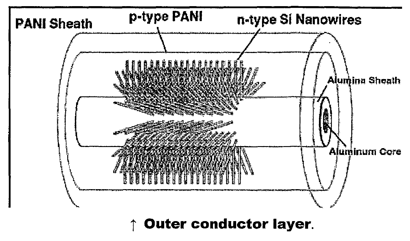
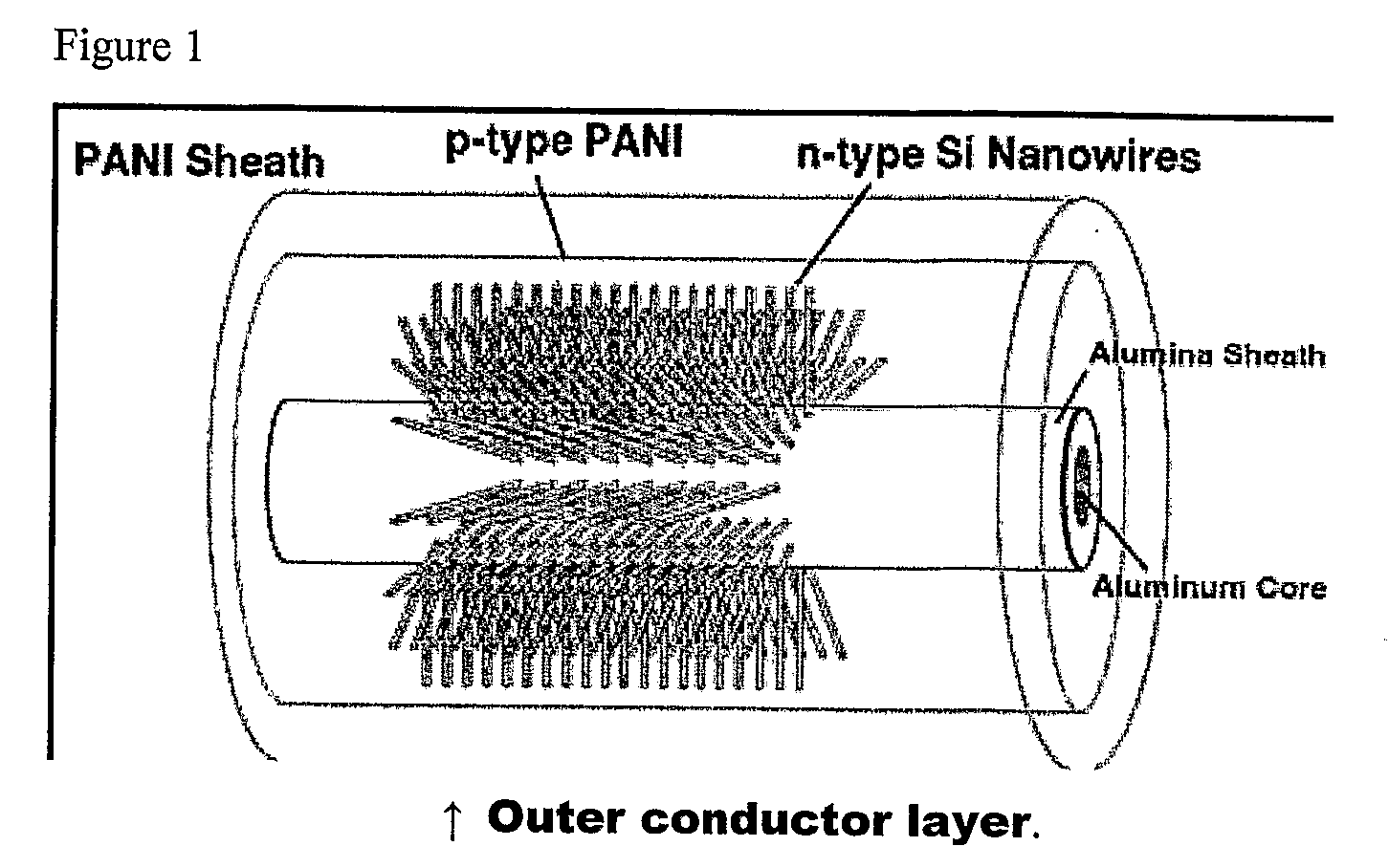
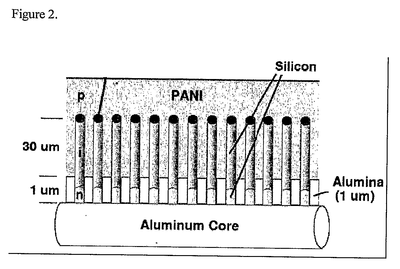
[0020]The photovoltaic wire invention presented here is produced by three basic steps: (1) producing a porous metallic oxide template structure on the surface of metallic wire or other substrate (2) inserting a catalytic seed in the oxide pores to initiate silicon nanowire formation of p, i (intrinsic), or n-type silicon nanowires, (3) growing the silicon nanowires out through the oxide pores, and (4) the application of n or p-type coating of polyaniline (PANI) or other similar conducting polymer to encase the silicon nanowire arrays and form a multitude of p-n junctions. In the preferred embodiment, the silicon nanow...


PUM

PropertyMeasurementUnit
diametersaaaaaaaaaa
diametersaaaaaaaaaa
thicknessaaaaaaaaaa

Abstract

A photovoltaic wire is presented where the active layers coat a metallic wire, preferably aluminum. The active layers are an array of doped silicon nanowires electrically attached to the metallic wire that extend from the surface of the wire into a layer of semiconducting polymer, preferably polyaniline. The surface of the polymer is coated with a transparent conductor to complete the photovoltaic circuit.

Description

[0001]This application claims priority to U.S. Pat. No. 60 / 692,026, filed on Jun. 17, 2005, which is incorporated herein by reference.[0002]This invention was supported in part by U.S. Government contract number 4200093584 awarded by NASA and portions of this invention may be subject to a paid-up license to the U.S. Government.BACKGROUND AND SUMMARY OF THE INVENTION[0003]The present invention relates generally to a nanostructured photovoltaic device that can be formed as a ribbon, wire or thread (referred to herein as PV wire). This device has numerous applications in the conversion of light into electrical energy. Photovoltaics, or solar cells, are a means of generating electricity directly from sunlight. The utilization of solar energy can have a tremendous influence on the quest for clean, renewable power sources that provide an alternative to the current fossil fuel based energy sources. The PV wire structure consists of electrically conductive wire core, preferably aluminum, wi...

Claims


Application Information

Patent Timeline
Patent Type & Authority Applications(United States)
IPC IPC(8): H01L31/0248H01L31/04C25D5/00H01L31/0352
CPCH01L27/301H01L27/304H01L51/0035H01L51/0036Y02E10/549H01L51/4213H01L51/4266H01L51/447H01L51/0038H10K30/53H10K39/10H10K85/114H10K85/113H10K85/111H10K30/352H10K30/10H10K30/87
Inventor HABIB, YOUSSEFSTEINBECK, JOHN
Owner ILLUMINEX CORP
Why Eureka
Try Eureka