Photoelectric conversion device and manufacturing method thereof

a technology manufacturing method, which is applied in the direction of semiconductor device, coating,plasma technique, etc., can solve the problems of low deposition rate, and low efficiency of photoelectric conversion device using microcrystalline silicon, so as to improve productivity, reduce the effect of change in characteristics and suppressing the effect of chang

Inactive Publication Date: 2009-11-12
SEMICON ENERGY LAB CO LTD
View PDF19 Cites 19 Cited by
  • Summary
  • Abstract
  • Description
  • Claims
  • Application Information

AI Technical Summary

Benefits of technology

[0009]As for photoelectric conversion devices using amorphous silicon thin films, the manufacturing process is simple and the cost can be reduced. However, they are not popular because the photoelectric conversion efficiency is lower than that of bulk photoelectric conversion devices and there is still a problem of photodegradation called Staebler-Wronski effect.
[0012]In view of the foregoing problems, an object of an embodiment of the present invention is to achieve the improvement in both efficiency and productivity of photoelectric conversion devices. Another object of an embodiment of the present invention is to provide a method for manufacturing photoelectric conversion devices having high efficiency by a simple manufacturing process. Another object of an embodiment of the present invention is to provide a photoelectric conversion device in which change in characteristics due to photodegradation or the like is prevented.
[0025]According to an embodiment of the present invention, a semiconductor layer in which a crystal region is included in an amorphous structure is formed as a main part for photoelectric conversion, so that the efficiency higher than that of conventional photoelectric conversion devices using amorphous silicon can be achieved. Further, with the semiconductor layer in which a crystal region is included in an amorphous structure, photodegradation or the like can be suppressed, so that change in characteristics can be suppressed as compared with conventional photoelectric conversion devices using amorphous silicon. Further, the thickness or the like of the photoelectric conversion layer can be as small as that of photoelectric conversion devices using amorphous silicon, whereby the productivity can be improved as compared with conventional photoelectric conversion devices using microcrystalline silicon. Accordingly, photoelectric conversion devices in which characteristics and productivity are both improved can be provided by the present invention.

Problems solved by technology

However, they are not popular because the photoelectric conversion efficiency is lower than that of bulk photoelectric conversion devices and there is still a problem of photodegradation called Staebler-Wronski effect.
However, since a microcrystalline silicon film is formed with the use of a semiconductor source gas typified by silane diluted with a large amount of hydrogen gas, there is a problem of low deposition rate.
For these reasons, photoelectric conversion devices using microcrystalline silicon are inferior in productivity to those using amorphous silicon.
In Patent Document 1, crystalline silicon (microcrystalline silicon is given as an example therein) is deposited with uniform crystallinity and film-quality by the control of pulse modulation in a high-frequency plasma CVD method; however, it is not practical because the deposition rate is low as compared with the deposition of amorphous silicon.
On the other hand, in Patent Document 2, the deposition rate is improved, but a silicon layer still needs to be thicker than in the case of using amorphous silicon by several digits; therefore, the problem in productivity remains unsolved.

Method used


Image

  • Photoelectric conversion device and manufacturing method thereof
  • Photoelectric conversion device and manufacturing method thereof
  • Photoelectric conversion device and manufacturing method thereof

Examples


embodiment 1

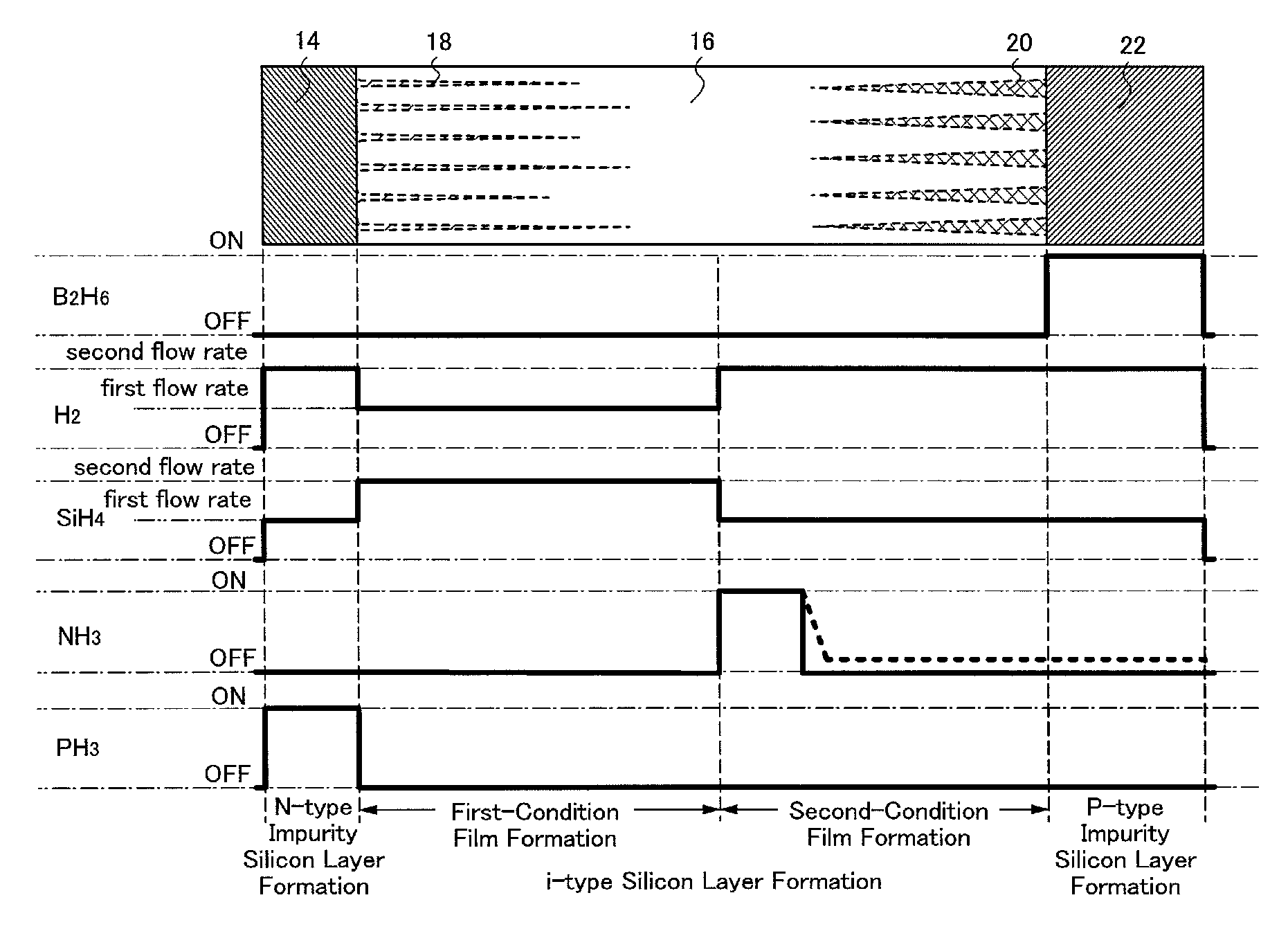
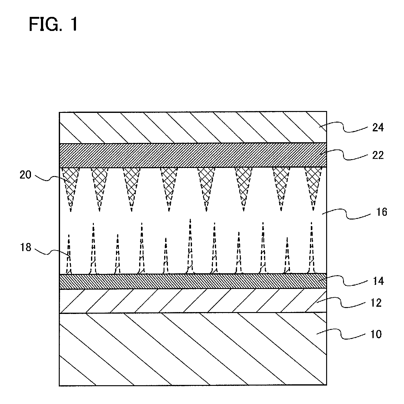
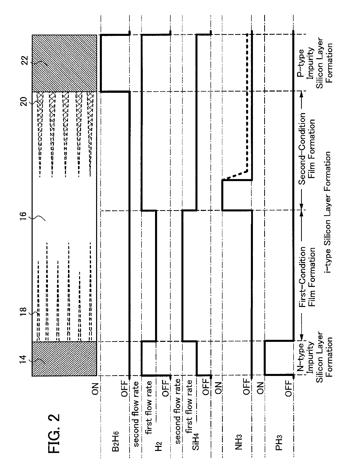
[0040]FIG. 1 shows a structure of a photoelectric conversion device according to Embodiment 1. The photoelectric conversion device shown in FIG. 1 includes a first electrode 12 provided over a substrate 10, a first semiconductor layer 14 provided over the first electrode 12, a second semiconductor layer 16 provided over the first semiconductor layer 14, a third semiconductor layer 22 provided over the second semiconductor layer 16, and a second electrode 24 provided over the third semiconductor layer 22. The first semiconductor layer 14 and the third semiconductor layer 22 are impurity semiconductor layers in which the conductivity types of impurity elements added thereto are opposite to each other; one is an n-type semiconductor layer and the other is a p-type semiconductor layer. The second semiconductor layer 16 provided between the first semiconductor layer 14 and the third semiconductor layer 22 is an i-type semiconductor layer in which a first crystal region and a second cryst...

embodiment 2

[0084]FIG. 5 illustrates the structure of a photoelectric conversion device according to Embodiment 2. The photoelectric conversion device includes at least one semiconductor junction by a second semiconductor layer 16 of an i-type semiconductor which is interposed between a first semiconductor layer 14 of an n-type semiconductor and a third semiconductor layer 22 of a p-type semiconductor. Shown here is the structure in which a low-concentration impurity semiconductor layer 13 is provided between the first semiconductor layer 14 and the second semiconductor layer 16. The low-concentration impurity semiconductor layer 13 is a semiconductor layer in which an impurity element imparting the same conductivity type as the first semiconductor layer 14 is contained and the impurity concentration is lower than that in the first semiconductor layer 14. Described in Embodiment 2 will be the example in which the low-concentration impurity semiconductor layer 13 is an n-type semiconductor.

[0085...

embodiment 3

[0093]In Embodiment 3, a so-called stack (including tandem) photoelectric conversion device in which a plurality of unit cells is stacked will be described. Described in Embodiment 3 will be the example of a photoelectric conversion device in which a unit cell including a single crystal semiconductor layer (typically single crystal silicon) and a unit cell including an amorphous semiconductor layer (typically non-single-crystal silicon) are included as a bottom cell and a top cell, respectively.

[0094]A photoelectric conversion device shown in FIG. 6 includes a first electrode 12 provided over a substrate 10 with an insulating layer 51 interposed therebetween, a unit cell 40 including a single crystal semiconductor layer, provided over the first electrode 12, a unit cell 30 including a non-single-crystal semiconductor layer, provided over the unit cell 40, and a second electrode 24 provided over the unit cell 30.

[0095]The unit cell 30 has a stack-layer structure of the first semicond...


PUM


Abstract

Higher conversion efficiency and productivity of photoelectric conversion devices. A semiconductor layer including a first and second crystal regions grown in the layer-deposition direction is provided between an impurity semiconductor layer containing an impurity element imparting one conductivity type and an impurity semiconductor layer containing an impurity element imparting a conductivity type opposite to the one conductivity type. The first crystal region is grown from the interface between one of the impurity semiconductor layers and the semiconductor layer. The second crystal region is grown toward the interface between the semiconductor layer and the other of the impurity semiconductor layers from a position which is away from the interface between the one of the impurity semiconductor layers and the semiconductor layer. The semiconductor layer including the first and second crystal regions which exist in an amorphous structure forms the main part of a region for photoelectric conversion.

Description

BACKGROUND OF THE INVENTION[0001]1. Field of the Invention[0002]The present invention relates to a photoelectric conversion device including a semiconductor junction and a method for manufacturing the photoelectric conversion device.[0003]2. Description of the Related Art[0004]To deal with global environmental issues in recent years, the market for photoelectric conversion devices typified by solar cells such as residential photovoltaic systems has expanded. Bulk photoelectric conversion devices using single crystal silicon or polycrystalline silicon, which have high photoelectric conversion efficiency, have already been put into practical use. The photoelectric conversion devices using single crystal or polycrystalline silicon are manufactured by cutting wafers from large silicon ingots. However, since it takes a long time to manufacture large silicon ingots, the productivity is low, and since supply of raw materials of silicon itself is limited, the supply of silicon ingots is in ...

Claims


Application Information

Patent Timeline
Patent Type & Authority Applications(United States)
IPC IPC(8): H01L31/0368H01L21/20
CPCH01L21/0262H01L31/03529Y02E10/50H01L31/0475H01L21/02532H01L21/02595H01L21/02529
Inventor YAMAZAKI, SHUNPEI
Owner SEMICON ENERGY LAB CO LTD
Why Eureka
Try Eureka