

Imaging Lens
a technology of imaging and lens, applied in the field of imaging lenses, can solve the problems of increasing the manufacturing cost including the cost of this heat-resistant socket, the inability to maintain optical performance, and the complicated manufacturing steps, so as to achieve the effect of high melting point, stable heat-resistant characteristic of the socket, and guaranteed optical performan
- Summary
- Abstract
- Description
- Claims
- Application Information
AI Technical Summary
Benefits of technology
Problems solved by technology
Method used
Image

Examples
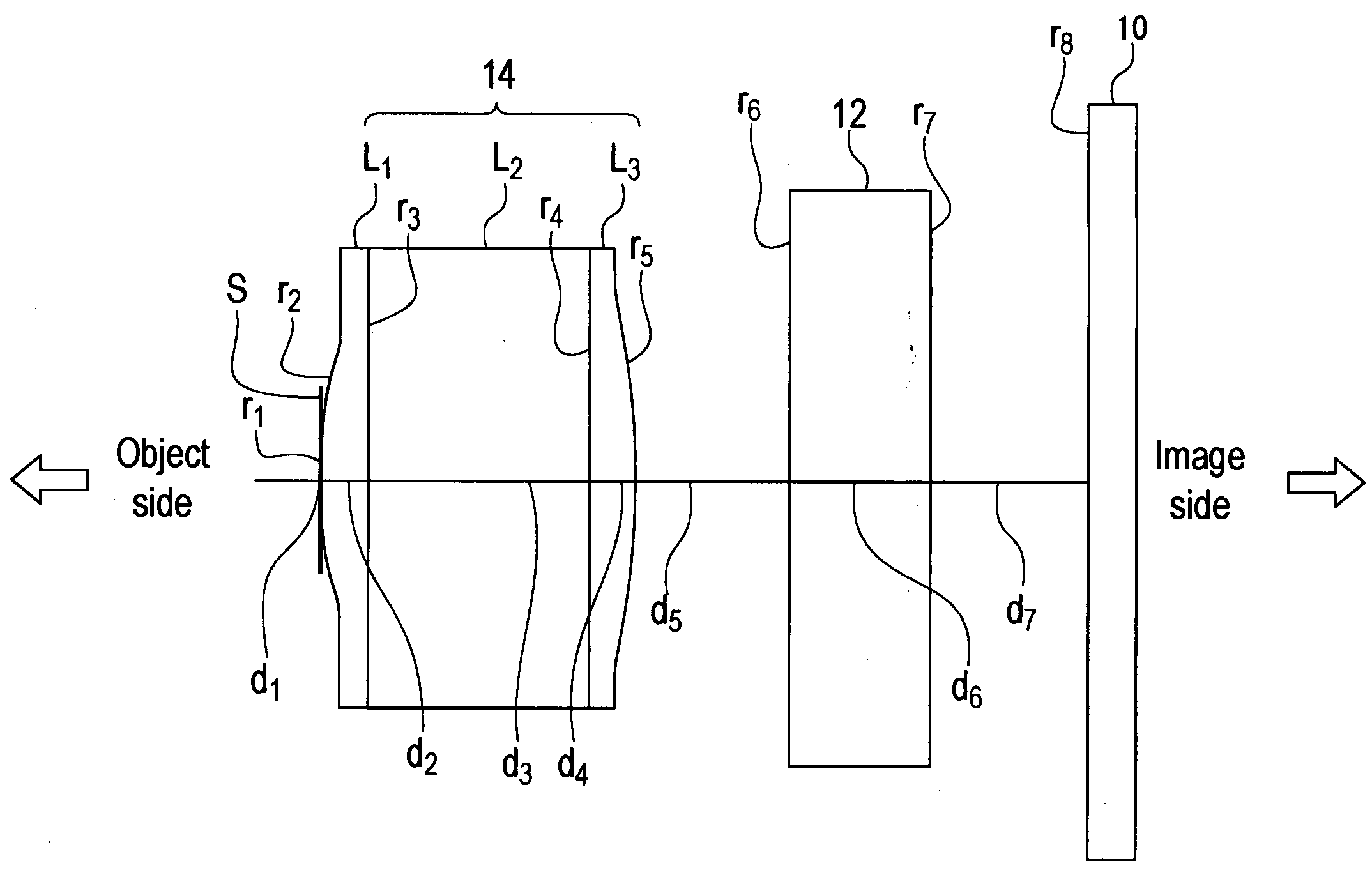
first embodiment
[0122]In the lens system of the first embodiment, the first lens L1 and the third lens L3 are formed of transparent high hardness silicone resin SMX-7852 (made by Fuji Polymer Industries Co., Ltd.) containing transparent adhesive, and the second lens L2 is formed by optical glass BK 7 (made by Ohara Inc.).
(A) The refractive index N2 of the first lens L1 is N2=1.51000.
(B) The refractive index N3 of the second lens L2 is N3=1.51680.
(C) The refractive index N4 of the third lens L3 is N4=1.51000.
(D) The Abbe number v2 of the first lens L1 is v2=56.0.
(E) The Abbe number v3 of the second lens L2 is v3=64.0.
(F) The Abbe number v4 of the third lens L3 is v4=56.0.
[0123]Therefore |N3−N2|=|N3−N4|=0.00680, which satisfies the following Conditions (1) and (2). Also |v3−v2|=|v3−v4|=8.0, which satisfies the following Conditions (3) and (4).
[0124]Conditions (1) and (2) refer to the conditions given by the following Expression (1) and (2). The conditions (3) and (4) refer to the conditions given by ...
second embodiment
[0135]In the lens system of the second embodiment, the first lens L1 and the third lens L3 are formed of transparent high hardness silicone resin SMX-7852 (made by Fuji Polymer Industries Co., Ltd.) containing transparent adhesive, and the second lens L2 is formed by optical glass BK 7 (made by Ohara Inc.).
(A) The refractive index N2 of the first lens L1 is N2=1.51000.
(B) The refractive index N3 of the second lens L2 is N3=1.51680.
(C) The refractive index N4 of the third lens L3 is N4=1.51000.
(D) The Abbe number v2 of the first lens L1 is v2=56.0.
(E) The Abbe number v3 of the second lens L2 is v3=64.0.
(F) The Abbe number v4 of the third lens L3 is v4=56.0.
[0136]Therefore |N3−N2|=|N3−N4|=0.00680, which satisfies the following Conditions (1) and (2). Also |v3−v2|=|v3−v4|=8.0, which satisfies the following Conditions (3) and (4).
[0137]FIG. 6 shows a cross-sectional view of the imaging lens of the second embodiment. As FIG. 6 shows, the aperture stop S is formed at a position of an inte...
third embodiment
[0146]In the lens system of the third embodiment, the first lens L1 and the third lens L3 are formed of transparent high hardness silicone resin IVSM-4500 (made by Toshiba Corporation) containing transparent adhesive, and the second lens L2 is formed by optical glass BK 7 (made by Ohara Inc.).
(A) The refractive index N2 of the first lens L1 is N2=1.42000.
(B) The refractive index N3 of the second lens L2 is N3=1.51680.
(C) The refractive index N4 of the third lens L3 is N4=1.42000.
(D) The Abbe number v2 of the first lens L1 is v2=52.0.
(E) The Abbe number v3 of the second lens L2 is v3=64.0.
(F) The Abbe number v4 of the third lens L3 is v4=52.0.
[0147]Therefore |N3−N2|=|N3−N4|=0.09680, which satisfies the following Conditions (1) and (2). Also |v3−v2|=|v3−v4|=12.0, which satisfies the following Conditions (3) and (4).
[0148]FIG. 10 shows a cross-sectional view of the imaging lens of the third embodiment. As FIG. 10 shows, the aperture stop S is formed at a position of an intersection of ...
PUM
 Abstract
Description
Claims
Application Information