Exposure mask using gray-tone pattern, manufacturing method of TFT substrate using the same and liquid crystal display device having the TFT substrate

a technology of tft substrate and exposure mask, which is applied in the direction of photomechanical treatment originals, instruments, optics, etc., can solve the problems of difficult control of the film thickness uniformity high cost of half tone mask, and difficulty in controlling the film thickness of the half film thickness part, etc., to reduce display defects, improve the uniformity of resist half film thickness, and improve the manufacturing yield

Inactive Publication Date: 2009-11-26
NEC LCD TECH CORP
View PDF0 Cites 9 Cited by
  • Summary
  • Abstract
  • Description
  • Claims
  • Application Information

AI Technical Summary

Benefits of technology

[0036]According to the invention, the light-shielding rate of the gray-tone area of the exposure mask is made to be higher at the longitudinal both ends of the light-shielding fine pattern than the center thereof, so that it is possible to improve the uniformity of the resist half film thickness on the substrate and to reduce the display defect, thereby improving the manufacturing yield.

Problems solved by technology

Since the semi-transparent film is used, the half tone mask is expensive.
However, the above processes using the gray-tone mask pattern need very precise control the process conditions.
Particularly, it is very difficult to control the film thickness uniformity of the half film thickness part.
As a result, the made channel length and shape of transistor is varied, which causes a problem on display.
Further, the resist film thickness of the half film thickness part is highly varied due to various factors such as resultant variation in the mask size, unevenness of each photolithography process and the like.
However, when the resist film thickness of the channel center is thicker than the end by a predetermined level or more, a part of the resist of the half film thickness part that should be removed by O2 ashing remains and metal pattern 41 of the channel part is shorted by the second etching of the metal layer (FIG. 5(a)), which cause point and line defects.
However, this method has an opposite effect with respect to the problems (FIGS. 5(a) to 5(c)) caused due to the fact that the resist film is thinner at the channel ends and thicker at the center, and cannot improve the uniformity of the resist film thickness, as shown in FIG. 4.
For this reason, the characteristics of the transistor are varied, so that display irregularities may be caused.
However, according to this method, the size of the semiconductor layer is too larger, so that an aperture ratio is lowered.
Thus, the above method does not have an effect to be expected.

Method used


Image

  • Exposure mask using gray-tone pattern, manufacturing method of TFT substrate using the same and liquid crystal display device having the TFT substrate
  • Exposure mask using gray-tone pattern, manufacturing method of TFT substrate using the same and liquid crystal display device having the TFT substrate
  • Exposure mask using gray-tone pattern, manufacturing method of TFT substrate using the same and liquid crystal display device having the TFT substrate

Examples


exemplary embodiment 1

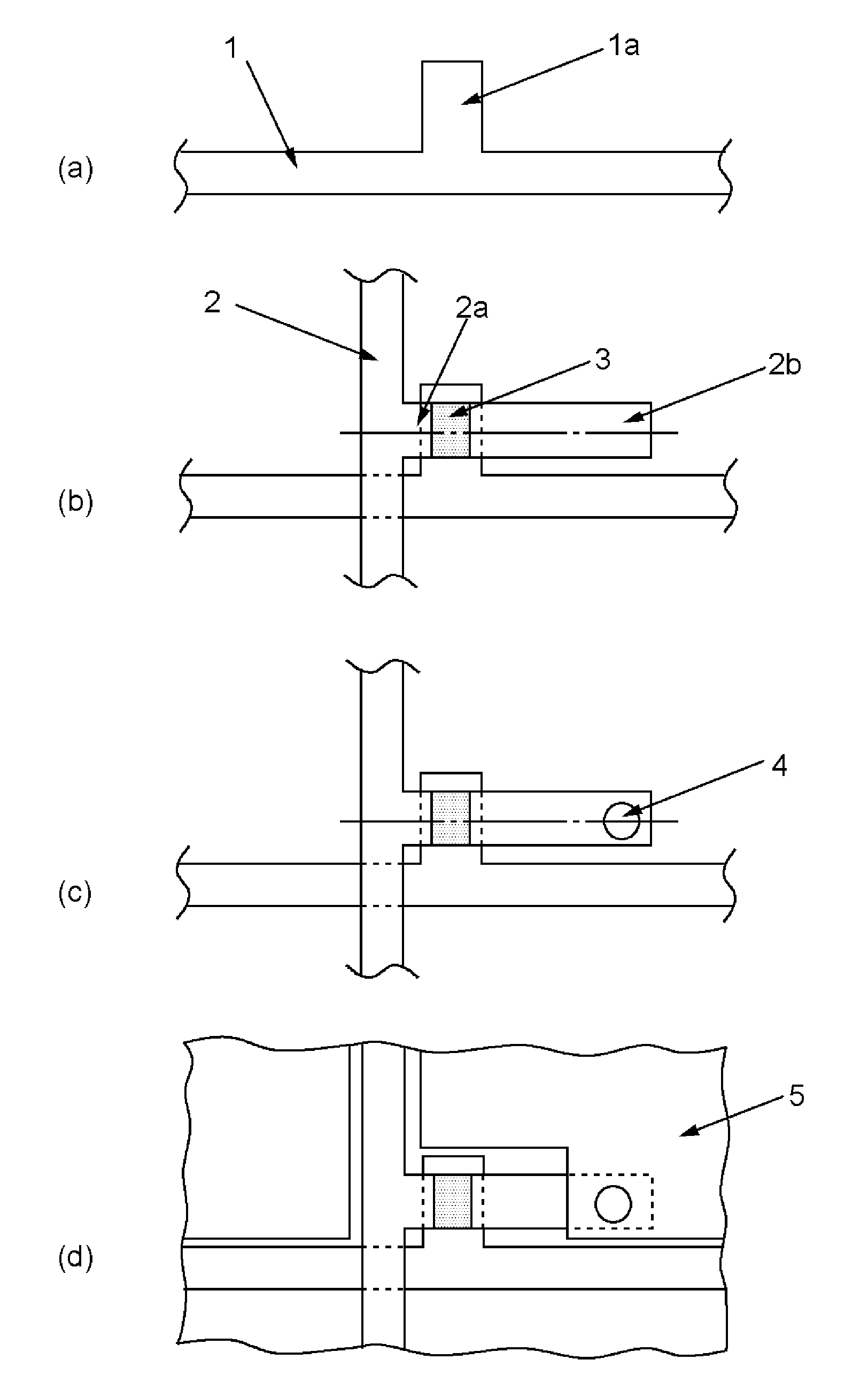
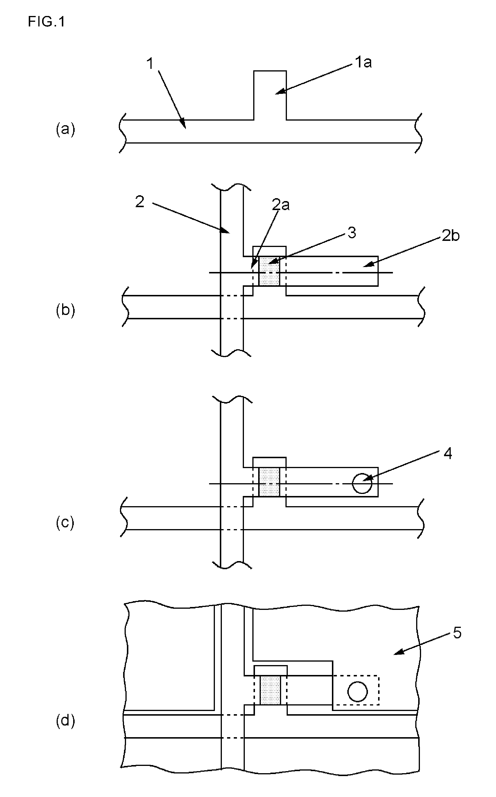
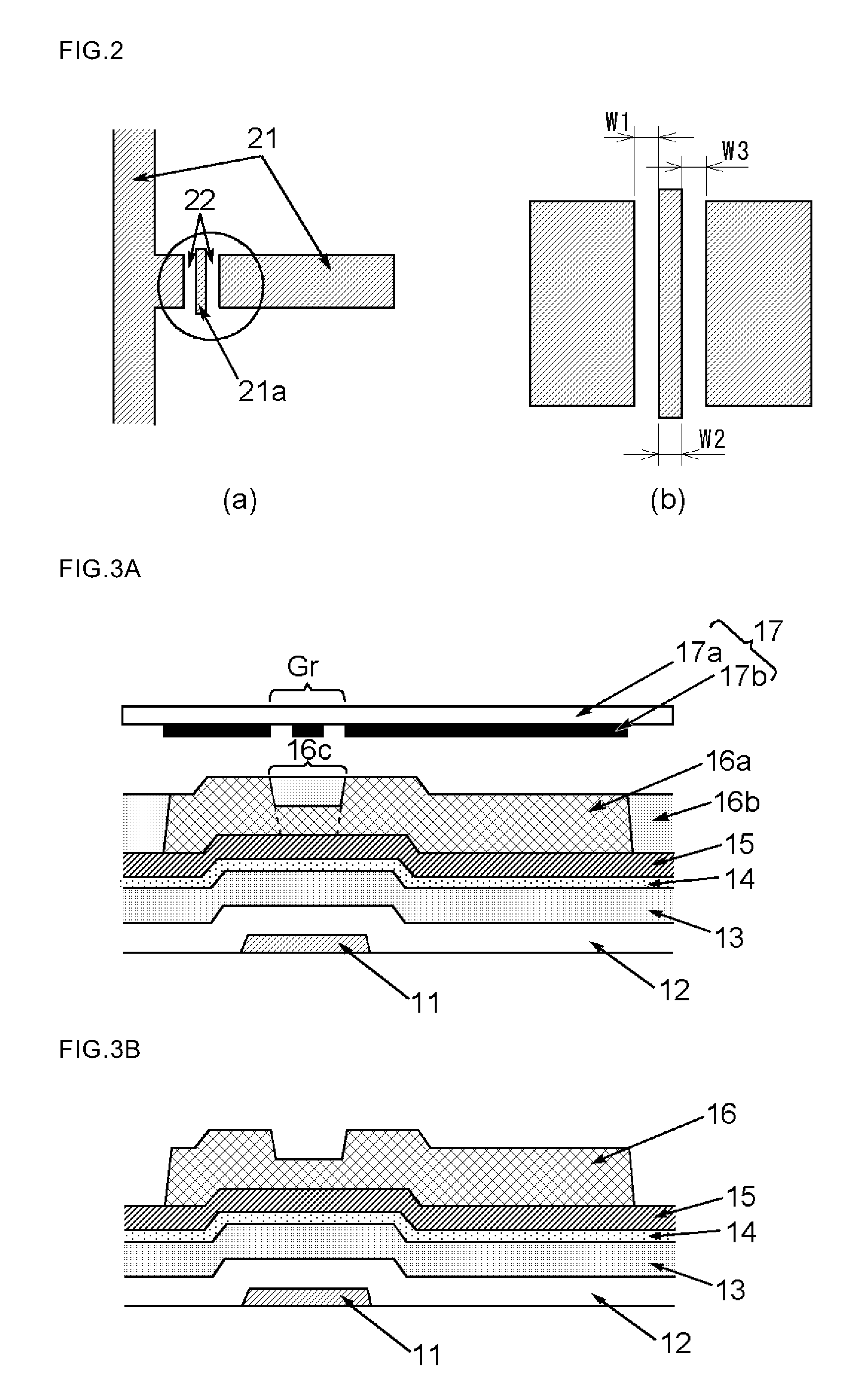
[0058]First, a film of metal such as Cr, Mo, Al or alloy thereof is formed on a transparent glass substrate and gate wiring 1, gate electrode 1a and a gate terminal (not shown) are formed in a first photolithography process (FIG. 1(a)). Then, as shown in a section view of FIG. 3A, SiNx film 12 to be a gate insulation film, a-Si layer 12 to be a semiconductor layer, n+a-Si layer 14 to be an ohmic contact layer, and metal layer 15 such as Cr, Mo, Al or alloy thereof are formed on gate electrode 11 by a CVD method and a sputtering method, respectively. Subsequently, a source electrode, a drain electrode, a drain wiring, a drain terminal (not shown) and an island are sequentially formed in a second photolithography process using a gray-tone mask.

[0059]The second photolithography process will be more specifically described. The second photolithography process uses a gray-tone mask. The gray-tone mask used in the second photolithography process has a gray-tone pattern arranged between sou...

exemplary embodiment 2

[0066]The liquid crystal display holds a liquid crystal layer between active matrix substrate 101 including a plurality of pixel electrodes formed thereon and opposite substrate 102 including opposite electrodes formed thereon. As shown in FIG. 11, active matrix substrate 101 includes a plurality of scanning lines (G1 to G9, xxx) and a plurality of data lines 104 (D1 to D9, xxx) arranged to intersect each other, and includes a plurality of pixel electrodes 105 arranged in areas surrounded by scanning lines 103 and data lines 104. Scanning lines 103 and data lines 104 are connected to pixel electrodes 105 via the pixel transistor as described in the exemplary embodiment 1.

[0067]In addition, a wiring pattern for a driving IC that is mounted in a COG or COF type is arranged in an area (P) of the vicinity of active matrix substrate 101. The wiring pattern is a control signal wiring and / or power supply wiring for a driving IC. The wiring pattern includes a plurality of wirings 108a, 108b...


PUM

PropertyMeasurementUnit
lengthaaaaaaaaaa
widthaaaaaaaaaa
width WCaaaaaaaaaa

Abstract

Disclosed are an exposure mask capable of improving uniformity of a resist film thickness of a half film thickness part and reducing a display defect to increase a manufacturing yield, a method of manufacturing a TFT substrate using the exposure mask and a liquid crystal display comprising the TFT substrate manufactured by the method and having no display defect. The exposure mask includes a light-shielding pattern on a transparent substrate in which a gray-tone area is provided to at least a part of the light-shielding pattern, the gray-tone area having an oblong light-shielding pattern having a width of a submarginal resolution of an exposure apparatus and sandwiched between oblong slit-type transmissive patterns having a width of the submarginal resolution, and a light-shielding rate of the gray-tone area is gradually reduced toward a center of the oblong light-shielding pattern from longitudinal ends thereof.

Description

[0001]This application is based upon and claims the benefit of priority from Japanese patent application No. 2008-131798, filed on May 20, 2008, the disclosure of which is incorporated herein in its entirety by reference.TECHNICAL FIELD[0002]The present invention relates to exposure mask using a gray-tone pattern capable of improving a thickness uniformity of thinner thickness resist film of a channel area (i.e., an area between source and drain electrodes) of a Thin Film Transistor (hereinafter, referred to as TFT) to enhance a manufacturing yield in a method of manufacturing a transistor array substrate for a liquid crystal display wherein source and drain wiring patterns and an island pattern of an active area are formed in a single photolithography process. The present invention also relates to a method of manufacturing an array substrate (TFT substrate) for a liquid crystal display using the exposure mask using a gray-tone pattern and a liquid crystal display having the TFT sub...

Claims


Application Information

Patent Timeline
Patent Type & Authority Applications(United States)
IPC IPC(8): H01L33/00G03F1/00H01L21/28G03F1/68G03F7/20H01L21/336H01L29/786
CPCG03F1/144H01L27/1214G03F1/36G03F1/50H01L27/1288
Inventor SAKURAI, HIROSHI
Owner NEC LCD TECH CORP
Why Eureka
Try Eureka