Low Inductance Ball Grid Array Device Having Chip Bumps on Substrate Vias

a technology of low inductance and chip bumps, applied in the direction of semiconductor devices, semiconductor/solid-state device details, electrical apparatus, etc., can solve the problems of reducing the electrical parameters of high-frequency bga devices, affecting the electrical parameters of devices, and affecting the application of flip-chip assemblies on substrates. achieve the effect of reducing electrical impedance, reducing bump-to-via current path inductance, and eliminating trace-to-trace coupling and trace-to-trace capa

Inactive Publication Date: 2009-11-26
TEXAS INSTR INC
View PDF3 Cites 41 Cited by
  • Summary
  • Abstract
  • Description
  • Claims
  • Application Information

AI Technical Summary

Benefits of technology

[0018]It is a technical advantage of the invention that of the traditional three signal interconnect structures from bumped chip terminal to package termination, namely bump pad, trace, and via (metal-filled through-hole topped by land), two structures are eliminated: bump pad and trace. This simplification eliminates trace-to-trace coupling and trace-to-trace capacitance, and reduces bump-to-via current path inductance from about 0.7 nH / mm to less than 0.1 nH / mm. It also reduces electrical impedance, and thus IR drop, for high frequency operation.
[0019]It is another technical advantage of the invention, that valuable real estate of the substrate area under the chip is freed up to be available for improved package routability, especially trace layout. In some devices, this savings avoids the need of requiring an additional routing layer—a significant cost savings.
[0020]As an additional technical advantage of the invention, the methodology is scalable. The approach of attaching the bumps of the high-frequency chip terminals directly on the substrate via can be used for more than one bump on a via, and it can also be extended to multi-layer substrates. This means that the electrical and cost advantages can be retained for several future fabrication nodes and product generations.
[0021]The technical advances represented by certain embodiments of the invention will become apparent from the following description of the preferred embodiments of the invention, when considered in conjunction with the accompanying drawings and the novel features set forth in the appended claims.

Problems solved by technology

Solder balls have, for practical reasons, relatively large diameters; consequently, when a device requires a great number of balls, the placement of the balls may necessitate substrates of an area considerably larger than the chip area.
The endeavour, however, to apply the flip-chip assembly on substrates to high-frequency BGA devices is running into severe problems.
For example, in the Digital Radio Processor (DRP) device families, the network of traces interconnecting the bumps on the traces, the vias, and the plating bar creates an unacceptable deterioration in electrical parameters.
In addition, in many devices is an increasing shortage of real estate for the layout of the interconnecting traces; the solution to use substrates with more than one metal layer is cost prohibitive.

Method used


Image

  • Low Inductance Ball Grid Array Device Having Chip Bumps on Substrate Vias
  • Low Inductance Ball Grid Array Device Having Chip Bumps on Substrate Vias
  • Low Inductance Ball Grid Array Device Having Chip Bumps on Substrate Vias

Examples


Embodiment Construction

[0031]The present invention is a continuation of U.S. patent application No. ______, filed on ______ Apr., 2008 (Rhyner et al., “BGA with One-Metal-Layer Substrate having Traces for Plating Pads under the Chip”).

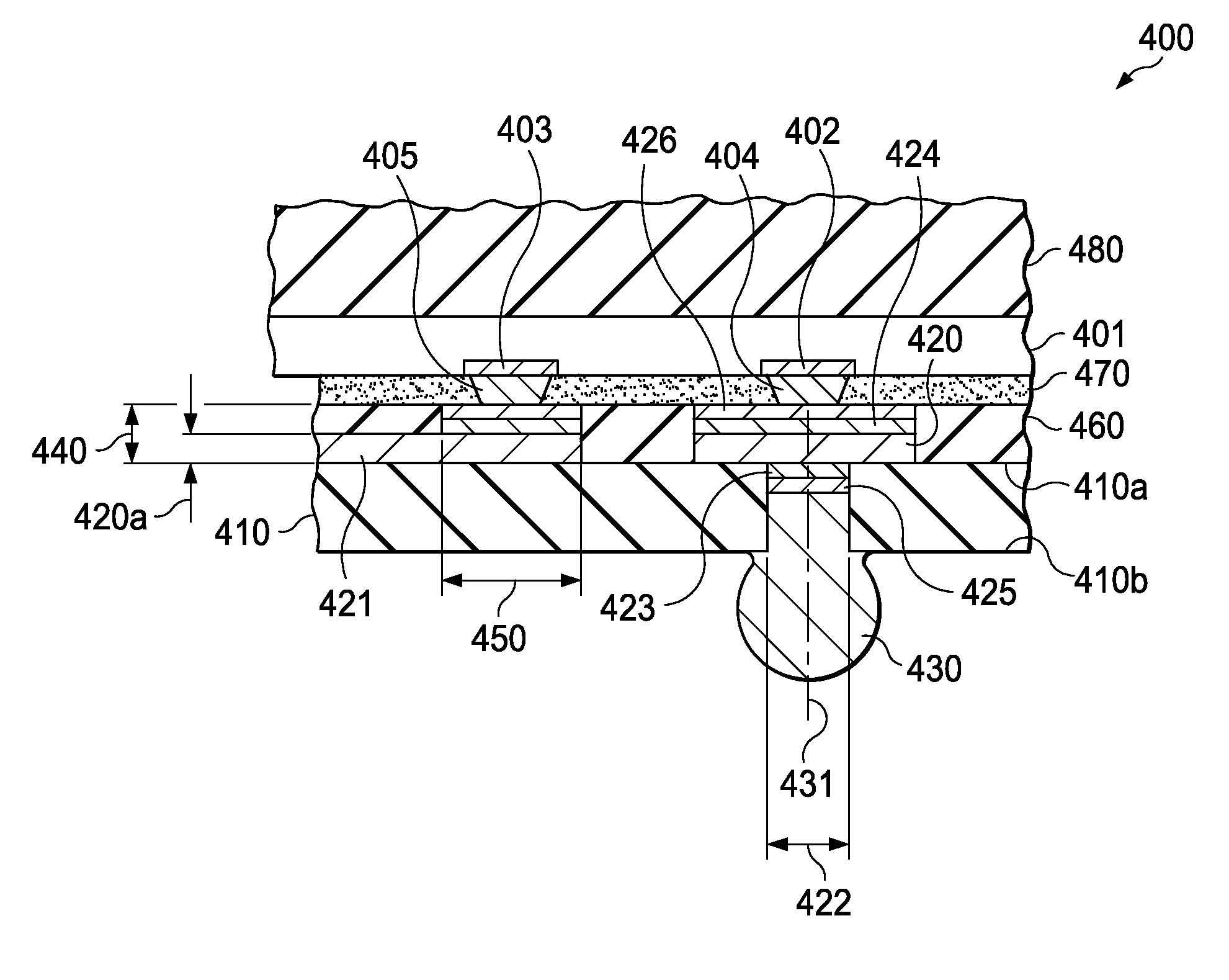
[0032]FIG. 4 illustrates an embodiment of the invention. FIG. 4 depicts a portion of an electronic device with a ball grid array (BGA) package, generally designated 400, which includes a semiconductor chip 401 with a first set of terminals 402 and a second set of terminals 403. In specific embodiments, chip 401 is an integrated circuit for Digital Radio Processor (DRP) devices, and the first set terminals 402 are high-frequency terminals. The second set terminals 403 serve low frequency signal inputs / outputs (I / O's), which have non-common net assignments. Chip 401 has additional terminals for power and ground, which have common net assignments and are not illustrated in FIG. 1. The chip terminals are preferably made of copper with a surface of gold or aluminum. Attached to t...


PUM


Abstract

A high-frequency BGA device (500) with the chip (501) assembled by metal bumps (503) on an insulating substrate (502) with conductive vias (505) and metal traces (504). Chip bumps which serve the high frequency signal terminals are attached directly to the lands (510) on the vias in order to minimize parasitic electrical parameters such as inductance, resistance, and IR drops, thus achieving the required 0.1 nH inductance for each chip terminal. Chip bumps which serve the remaining chip terminals are attached to pads on certain substrate traces. In both cases, the bumps can be attached reliably because the lands on the vias and the pads on the traces are plated with additional metal layers (511, 512), which provide extra thickness as well as a metallurgically suitable surface.

Description

FIELD OF THE INVENTION[0001]The present invention is related in general to the field of semiconductor devices and processes, and more specifically to the structure and electrical characteristics of ball grid array packages suitable for high-speed electrical devices.DESCRIPTION OF RELATED ART[0002]In the popular ball-grid-array (BGA) packages of electronic devices, the semiconductor chip is assembled on an insulating substrate, typically in the central region. The substrate has at least one metal layer, usually a thin copper foil, which is patterned into lands, such as contact pads, and interconnecting traces. Electrically conductive through-holes (so-called vias) extend through the substrate thickness to connect the lands on one surface to solder pads on the opposite surface, where solder balls are attached in order to handle the connection to external parts. Solder balls have, for practical reasons, relatively large diameters; consequently, when a device requires a great number of ...

Claims


Application Information

Patent Timeline
Patent Type & Authority Applications(United States)
IPC IPC(8): H01L23/498H01L21/60
CPCH01L21/563H01L2224/16235H01L23/49811H01L23/49816H01L23/49827H01L23/49838H01L23/49866H01L23/66H01L24/16H01L24/17H01L2223/6616H01L2223/6622H01L2224/13099H01L2224/16225H01L2224/73203H01L2224/73204H01L2924/01002H01L2924/01013H01L2924/01029H01L2924/01075H01L2924/01077H01L2924/01078H01L2924/01079H01L2924/01082H01L2924/14H01L2924/15311H01L2924/30105H01L2924/30107H01L2924/3011H01L2924/3025H01L2924/01033H01L23/3128H01L24/05H01L2224/05147H01L2224/05571H01L2224/05573H01L2224/05624H01L2224/05644H01L2224/16106H01L2924/181H01L2924/00H01L2924/00014
Inventor RHYNER, KENNETH R.HARPER, PETER R.
Owner TEXAS INSTR INC
Why Eureka
Try Eureka