Semiconductor Saturable Absorber Reflector and Method to Fabricate Thereof

a saturable absorber and reflector technology, applied in the field of saturable absorber absorber devices of semiconductors, can solve the problems of relaxation of the crystalline structure in the absorbing region, and achieve the effect of accurately modified and controlled absorption recovery tim

Active Publication Date: 2009-12-03
OPTOELECTRONICS RES CENT
View PDF6 Cites 11 Cited by
  • Summary
  • Abstract
  • Description
  • Claims
  • Application Information

AI Technical Summary

Benefits of technology

[0008]According to this invention, the absorption recovery time is controlled during the epitaxial growth by using lattice-mismatched layer(s) to induce dislocations, i.e. misfit and threading dislocations, and implicitly non-radiative recombination centers within the nonlinear absorbing region. A very important feature of the invention consist in a relaxation of the design constrains for the active region; the thickness of the active region can be largely varied while the number of the dislocations can be accurately modified during the fabrication. The general architecture of the device comprises a distributed Bragg reflector (DBR) lattice matched to a semiconductor substrate, lattice reformation layer(s), the nonlinear absorption region, containing quantum-wells, quantum-dots or bulk semiconductor material, and a cap layer. Depending on the design approach, i.e. operation wavelength and choice of material, the nonlinear layer is either lattice-matched or lattice-mismatched to the substrate and the DBR material. The lattice reformation layer(s) grown between DBR and the absorber is an instrumental to control the amount of dislocations and implicitly the amount of non-radiative recombination centers used to trap the optically excited carriers generated in the absorption region.

Problems solved by technology

If the nonlinear layer and the DBR material are largely mismatched then the number of defects in the nonlinear region could be very high eventually resulting in relaxation of the crystalline structure in the absorbing region.

Method used


Image

  • Semiconductor Saturable Absorber Reflector and Method to Fabricate Thereof
  • Semiconductor Saturable Absorber Reflector and Method to Fabricate Thereof
  • Semiconductor Saturable Absorber Reflector and Method to Fabricate Thereof

Examples


Embodiment Construction

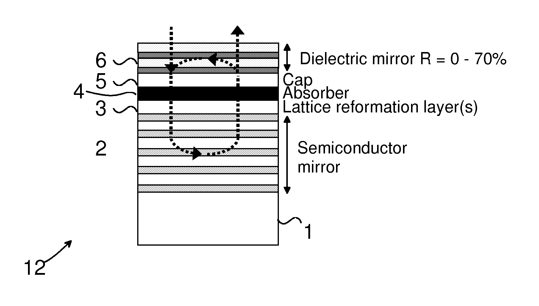
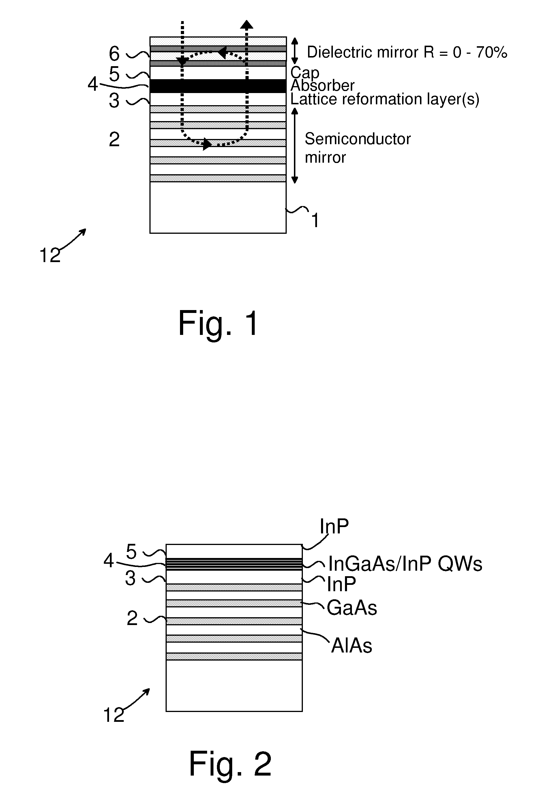
[0028]With reference to FIG. 1, the general structure of a semiconductor saturable absorber designed according to this invention includes a semiconductor substrate 1, for example GaAs or InP, suitable for growing high quality compound semiconductors with alternate high and low refractive indices to form the distributed Bragg reflector 2. The DBR layers have thicknesses of a quarter of the optical wavelength at which the DBR is designed to have a maximum reflection. Reflectivity can be adjusted by changing the number of constituting layers. The lattice reformation section 3 comprises semiconductor layer(s) with a lattice constant different from that of the DBR layers to manage the process of generating defects in the crystalline structure. The device includes the absorbing multi-layers region 4 comprising layer(s) with energy band-gap small enough to absorb an optical signal and provide a nonlinear interaction with the signal. Depending on the operating wavelength and other desired f...


PUM


Abstract

A design of a semiconductor saturable absorber that offers a convenient and reliable way to control/decrease the recovery time of the absorption. The absorption recovery time is controlled during the epitaxial growth by using lattice-mismatched layer(s) to induce dislocations, and implicitly non-radiative recombination centers within the nonlinear absorbing region. These lattice reformation layer(s) are interposed between the distributed Bragg reflector and the nonlinear absorption region, containing quantum-wells, quantum-dots or bulk semiconductor material. The thickness and composition of the lattice reformation layer(s) is an instrumental to control the amount of non-radiative recombination centers used to trap the optically excited carriers generated in the absorption region.

Description

FIELD OF THE INVENTION[0001]The present invention relates generally to semiconductor devices comprising saturable absorbers, and in particular to a concept to reduce the recovery time of absorption, a method to fabricate thereof, and the use of such a device in mode-lock lasers. The method also relates to a method for manufacturing a semiconductor device comprising forming a distributed Bragg reflector layer on a semiconductor substrate, forming an absorption region, and forming a cap layer on the absorption region. The method further relates to a laser comprising a gain medium, means to pump the gain medium, a mirror, one or more dispersion compensating elements, and a semiconductor device comprising a semiconductor substrate, a distributed Bragg reflector layer, an absorption region, and a cap layer.BACKGROUND OF THE INVENTION[0002]Semiconductor saturable absorbers are nonlinear optical elements that impose an intensity-dependent attenuation on a light beam incident upon it; an in...

Claims


Application Information

Patent Timeline
Patent Type & Authority Applications(United States)
IPC IPC(8): H01S5/00H01L21/00
CPCB82Y10/00B82Y20/00G02F1/3523G02F2201/346H01S3/113G02F2202/102G02F2202/108H01S3/08059H01S3/1118G02F2202/101
Inventor OKHOTNIKOV, OLEGGUINA, MIRCEAGRUDININ, ANATOLY B.
Owner OPTOELECTRONICS RES CENT
Why Eureka
Try Eureka