
IC tag label

a technology of ic tags and labels, applied in the field of ic tags, can solve the problems of low cost, frequent exposure to unavoidable external stress, fatal damage, etc., and achieve the effect of avoiding an increase in the thickness of the ic chip section, increasing material cost and production cos

Active Publication Date: 2009-12-10
DAI NIPPON PRINTING CO LTD
View PDF2 Cites 8 Cited by
  • Summary
  • Abstract
  • Description
  • Claims
  • Application Information

AI Technical Summary

Benefits of technology

[0018]The IC tag label according to the present invention is such that the clearance for the IC chip is provided in the IC chip protection sheet to avoid an increase in the thickness of the IC chip section. Therefore, the IC chip is not likely to become damaged when it receives an external impact. Further, the IC tag label according to the present invention does not increase the material cost and production cost because it can be manufactured without any additional particular material unlike an IC tag label having a conventional configuration.
[0019]Furthermore, even when the IC tag label according to the present invention is in the form of a continuously wound product, the IC chip does not become damaged due to strong pressure that is exerted by winding during manufacture or after completion of production.

Problems solved by technology

However, when a noncontact IC tag label is used as a distribution label, it is frequently exposed to unavoidable external stress.
It is fatally damaged particularly if its IC chip section receives an impact.
However, such a structure was complicated so that noncontact IC tags could not be manufactured at a low cost.
An unavoidable structural problem of noncontact IC tag labels is that IC chips are much greater in thickness than an employed substrate and other parts.
It is conceivable that IC chips may become damaged when they are stacked.
If, in such an instance, a heavy object is placed on top of the labels, any one of the vertically-aligned adjacent IC chips are impacted so that the IC chips containing a silicon crystal are damaged.
In this case, the labels, although they are unused, are suspected of being defective.
The IC tag label disclosed in Patent Document 1 entails an increased production cost because of the material cost of the structure and the difficulty in inserting the structure into its position.

Method used


Image

  • IC tag label
  • IC tag label
  • IC tag label

Examples


first embodiment

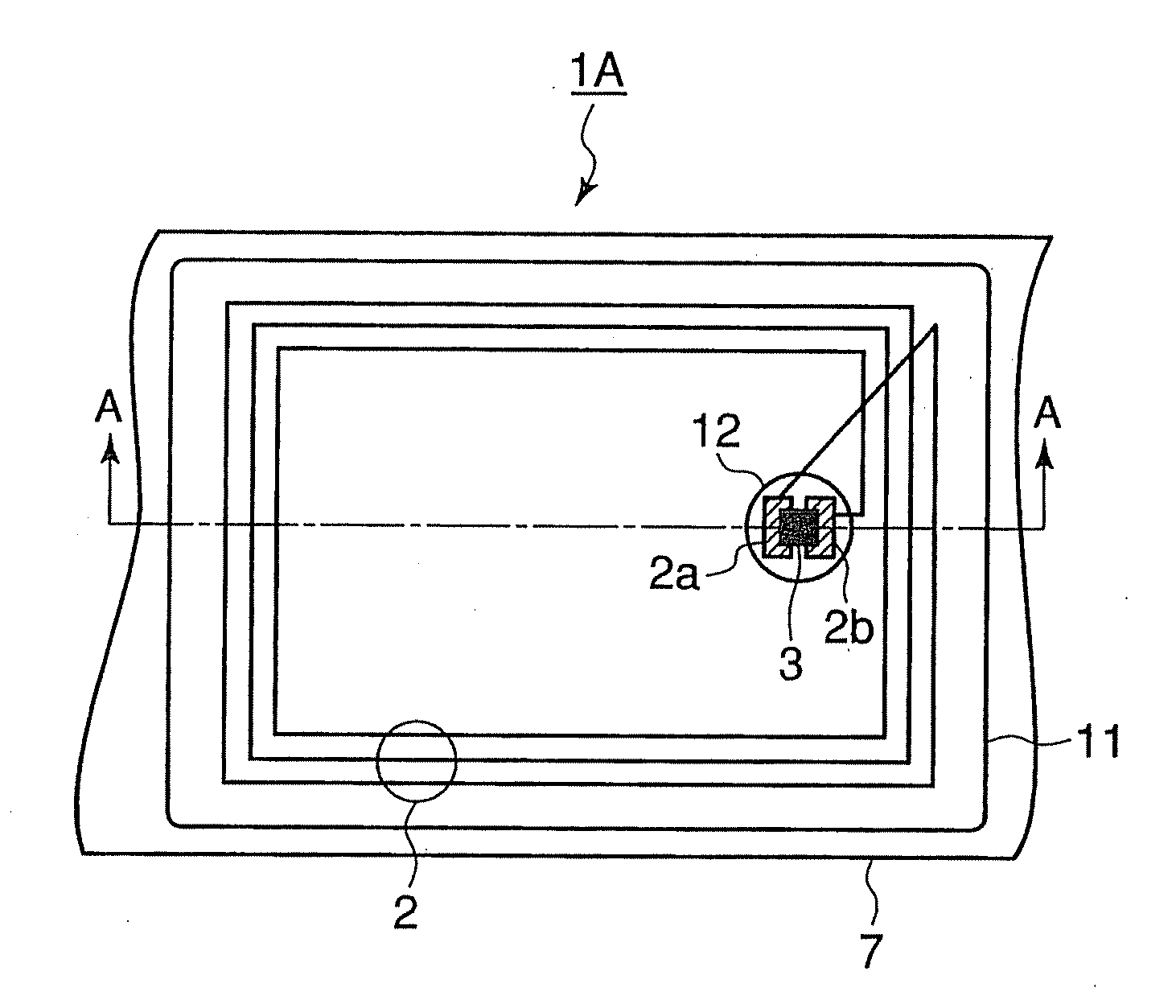
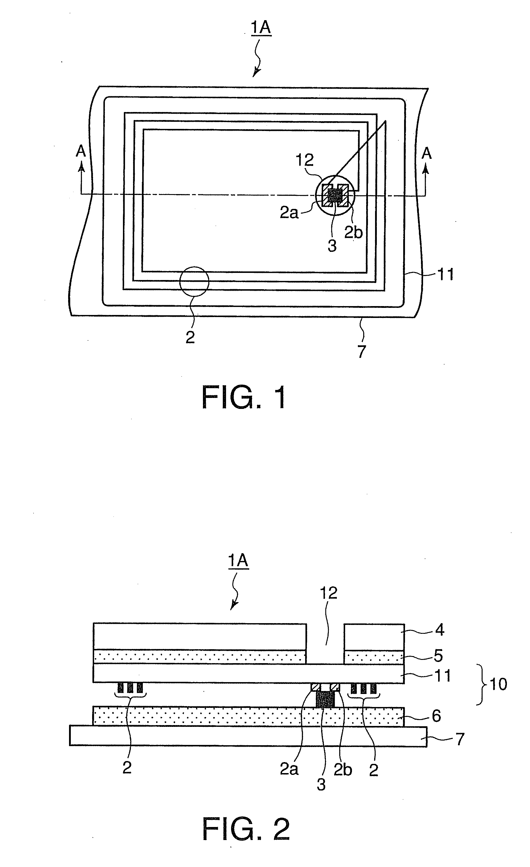
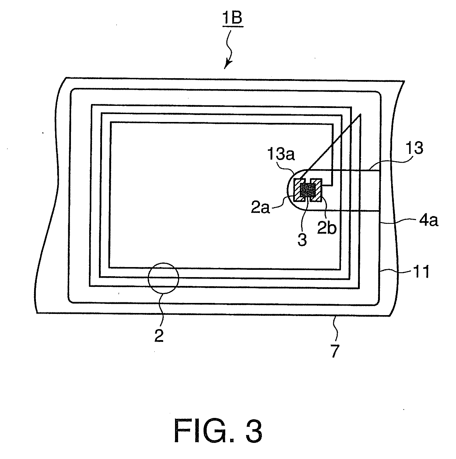
[0028]Modes of a first embodiment of the present invention will now be described sequentially with reference to the accompanying drawings. FIG. 1 is a plan view illustrating an IC tag label according to mode 1-1 of the first embodiment. FIG. 2 is a cross-sectional view taken along line A-A in FIG. 1. FIG. 3 is a plan view illustrating the IC tag label according to mode 1-2 of the first embodiment. FIGS. 4(A) to 4(E) are diagrams illustrating a manufacturing process for the IC tag label according to mode 1-1 of the first embodiment. FIGS. 5(A) to 5(E) are diagrams illustrating a manufacturing process for the IC tag label according to mode 1-2 of the first embodiment. FIG. 6 is an external view of an inlet having a coil antenna.

[0029]As shown in FIGS. 1 and 2, the IC tag label 1A according to mode 1-1 of the first embodiment includes an inlet substrate 11; an IC chip protection sheet 4, which is mounted on the whole of one surface of the inlet substrate 11 via a protection sheet bond ...

example 1 of first embodiment

(Preparing the Inlet)

[0055]A transparent biaxially-stretched polyethylene terephthalate (PET) film, which was 65 mm wide and 20 μm thick, was used as the inlet substrate 11. A 25 μm thick aluminum foil was dry-laminated to the inlet substrate 11 to produce a web material. A print resist was then used to print a coiled antenna pattern onto the web material. Next, etching was conducted to mount the conductive member 8 and complete the antenna pattern 2 shown in FIG. 6. The external size of the antenna pattern 2 was such that it measured approximately 45 mm by 76 mm. A plurality of antenna patterns 2 were disposed at intervals of 88 mm. The IC chip 3 having a planar size of 1.0 mm square, a thickness of 120 μm, and a spike-like bump was mounted in a face-down manner on both ends 2a, 2b of the antenna pattern 2 under thermal pressure to complete the inlet 10 in a continuous strip form (FIG. 4(A)).

(Preparing the IC Chip Protection Sheet)

[0056]A PET sheet measuring 65 mm wide and 40 μm th...

example 2 of first embodiment

(Preparing the Inlet)

[0058]A transparent biaxially-stretched PET film, which was 65 mm wide and 20 μm thick, was used as the inlet substrate 11. A 25 μthick aluminum foil was dry-laminated to the inlet substrate 11 to produce a web material. The same process was performed on the web material as described in connection with Example 1 of the first embodiment to complete the inlet 10 in a continuous strip form (FIG. 5(A)). The same IC chip 3 was used as in Example 1 of the first embodiment.

(Preparing the IC Chip Protection Sheet)

[0059]A resin-coated paper measuring 70 mm wide and 60 μm thick (this thickness includes the thickness of a 20 μm thick adhesive layer 5) was used as the IC chip protection sheet 4. A cut-out 13 composed of a 4 mm diameter semicircle and a 4 mm wide groove following the semicircle was made at the position of the IC chip protection sheet 4 corresponding to the IC chip 3 of the inlet 10. A plurality of cut-outs 13 were disposed at intervals of 88 mm (see FIG. 3)....


PUM

PropertyMeasurementUnit
thicknessaaaaaaaaaa
thicknessaaaaaaaaaa
thicknessaaaaaaaaaa

Abstract

An IC tag label 1A includes an inlet substrate 11; an IC chip protection sheet 4 which is mounted on one surface of the inlet substrate 11; and an antenna pattern 2 and an IC chip 3 which are mounted on the other surface of the inlet substrate. An adhesive layer is mounted on the other surface of the inlet substrate 11 to cover the antenna pattern 2 and IC chip 3. An opening, which serves as a clearance for the IC chip 3, is formed in a portion of the IC chip protection sheet 4, the portion corresponding to the IC chip 3.

Description

TECHNICAL FIELD[0001]The present invention relates to an IC tag label that is structured to avoid damage to an IC chip. More specifically, the present invention relates to an IC tag label that is used, for instance, as a shipping tag attached to a baggage, packing case, or the like, a merchandise label, a product management tag, a voucher, or the like, and structured to reduce the protrusion height of an IC chip section.[0002]The present invention is mainly applicable to the manufacture or use of IC tag labels and, more specifically, to such categories as transportation, distribution, inventory control, and plant process control of IC tag labels.BACKGROUND ART[0003]Noncontact IC tag labels are now frequently used as recognition media in the fields, for instance, of transportation and distribution, or used for product quality control, inventory control, and various other purposes because they can record and retain information and establish noncontact communication to exchange the inf...

Claims


Application Information

Patent Timeline
Patent Type & Authority Applications(United States)
IPC IPC(8): H04Q5/22
CPCG06K19/07722Y10T156/1077G06K19/07749
Inventor OGATA, TETSUJI
Owner DAI NIPPON PRINTING CO LTD
Learn More