

Chemical trim of photoresist lines by means of a tuned overcoat material
a technology of photoresist line and overcoat, which is applied in the direction of photosensitive materials, instruments, photomechanical equipment, etc., can solve the problems of too much activation of resist, too much reduction in linewidth, and acid will not provide sufficient activation of resist to provide enough reduction in resist linewidth. , to achieve the effect of superior linewidth control and reducing the linewidth of an imag
- Summary
- Abstract
- Description
- Claims
- Application Information
AI Technical Summary
Benefits of technology
Problems solved by technology
Method used
Image

Examples
Embodiment Construction
[0001]1. Field of the Invention
[0002]The field of the invention comprises formation of fine line lithography patterns for the purpose of semiconductor fabrication.
[0003]2. Background of the Invention and Related Art
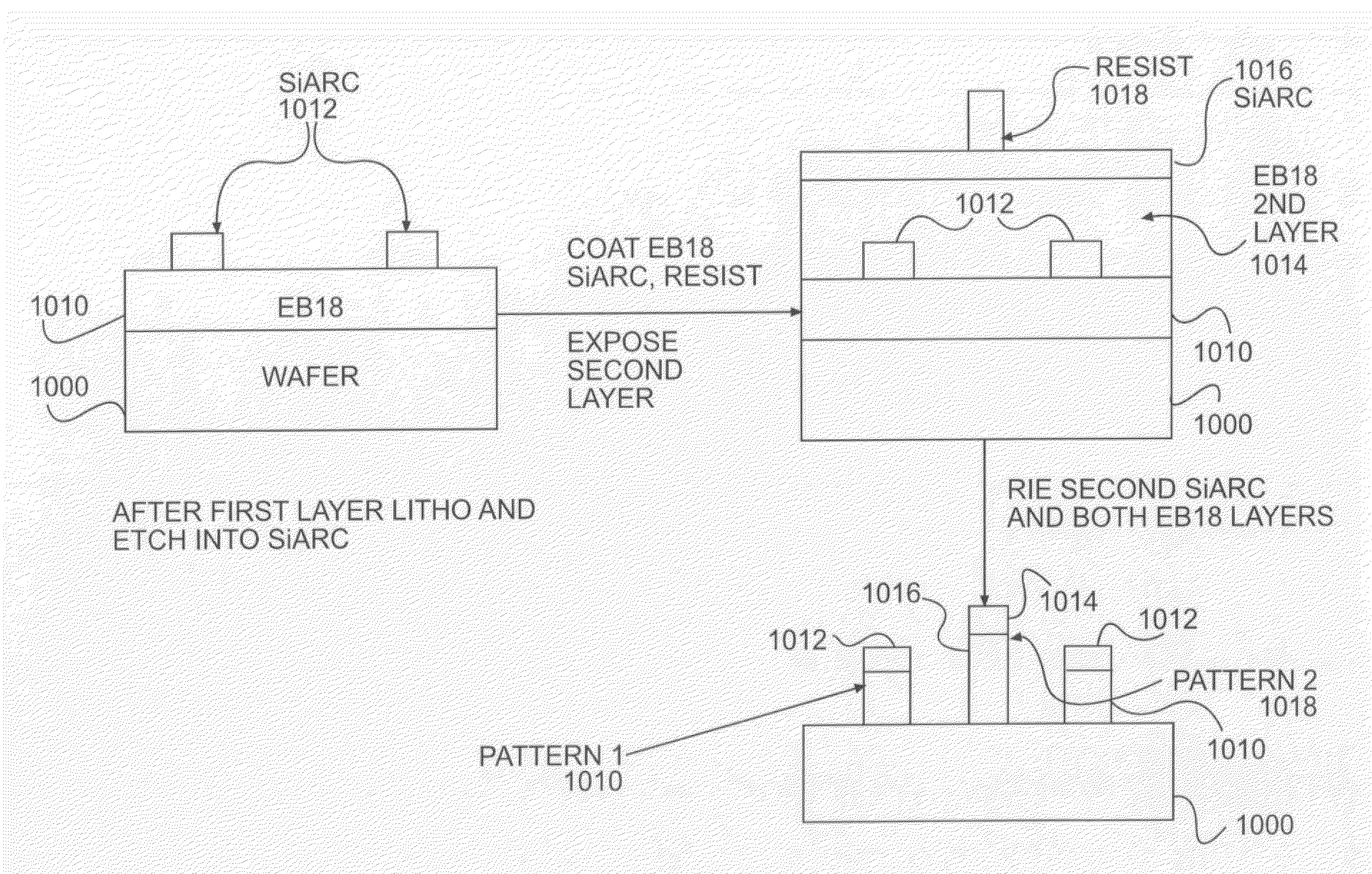
[0004]Historically, lithographic scaling has generally been achieved by means of increasing the numerical aperture available for optical exposure equipment, and by means of using shorter exposure wavelengths. At present, the industry has reached a condition in which it is no longer possible to economically increase numerical aperture or reduce the exposure wavelength. As a result, many alternative methods of scaling integrated circuit lithography are being investigated. One method involves the use of multiple exposures to form a single lithographic mask pattern on the wafer. The pitch of the pattern is split by interstitially placing a line from a second mask in between two lines formed by a first mask. The effective pitch of the resulting combined pattern can be twice as...
PUM
| Property | Measurement | Unit |
|---|---|---|
| temperature | aaaaa | aaaaa |
| temperature | aaaaa | aaaaa |
| temperature | aaaaa | aaaaa |
Abstract
Description
Claims
Application Information