Thin film transistor, method of manufacturing the same, and flat panel display device haviing the same

a technology of thin film transistors and flat panels, which is applied in the direction of transistors, semiconductor devices, electrical devices, etc., can solve the problems of increasing manufacturing costs, decreasing yield, and difficult to operate driving circuits at high speeds, so as to improve the ohmic contact characteristics of an oxide semiconductor layer and a metal electrod

Inactive Publication Date: 2009-12-24
SAMSUNG DISPLAY CO LTD
View PDF15 Cites 75 Cited by
  • Summary
  • Abstract
  • Description
  • Claims
  • Application Information

AI Technical Summary

Benefits of technology

[0010]Aspects of the present invention provide a thin film transistor, a method of manufacturing the same, and a flat panel display device having the same capable of improving ohmic contact characteristics of an oxide semiconductor layer and a metal electrode.

Problems solved by technology

However, if the active layer is formed of amorphous silicon, the active layer has low mobility so that it is difficult to operate a driving circuit at a high speed.
Also, if the active layer is formed of poly-silicon, the active layer has a high mobility but a non-uniform threshold voltage so that a separate compensation circuit is necessary.
Accordingly, a complicated process and a number of masks are used thus increasing manufacturing cost and decreasing yield.
However, a conventional thin film transistor using the oxide semiconductor as the active layer has poor ohmic contact with a metal electrode due to a wide band gap of the oxide semiconductor.

Method used


Image

  • Thin film transistor, method of manufacturing the same, and flat panel display device haviing the same
  • Thin film transistor, method of manufacturing the same, and flat panel display device haviing the same
  • Thin film transistor, method of manufacturing the same, and flat panel display device haviing the same

Examples


Embodiment Construction

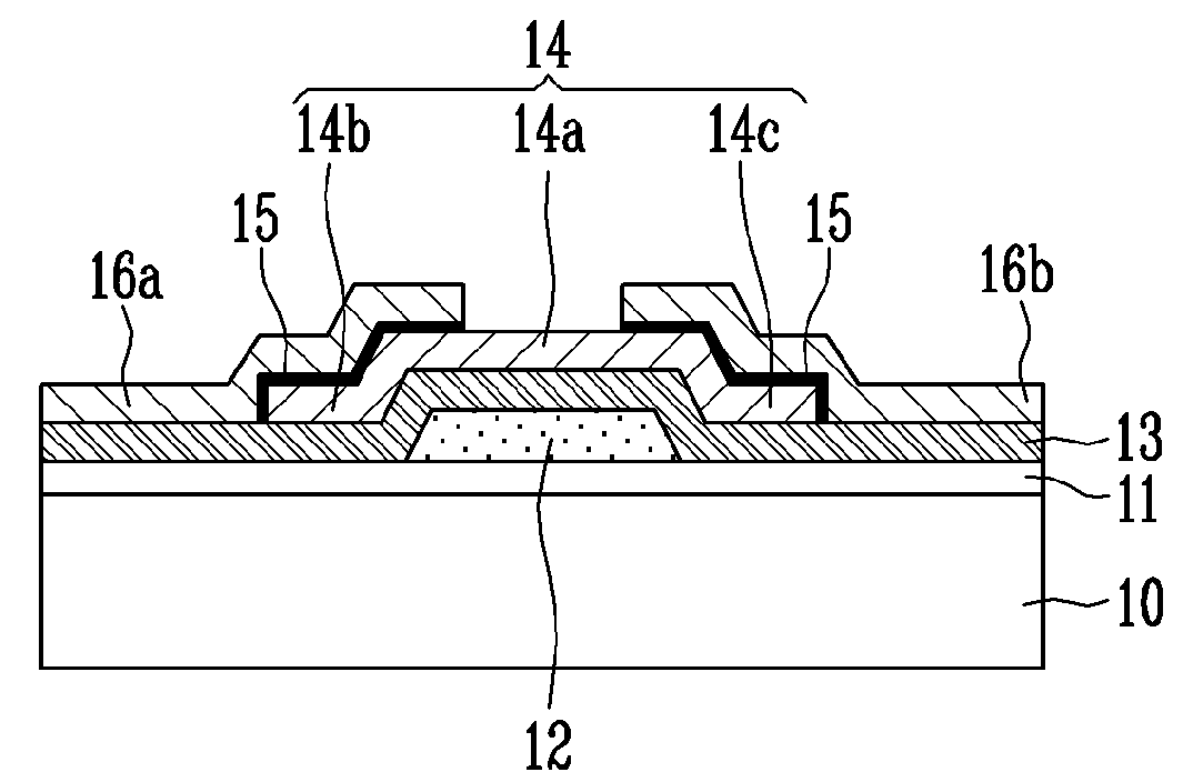
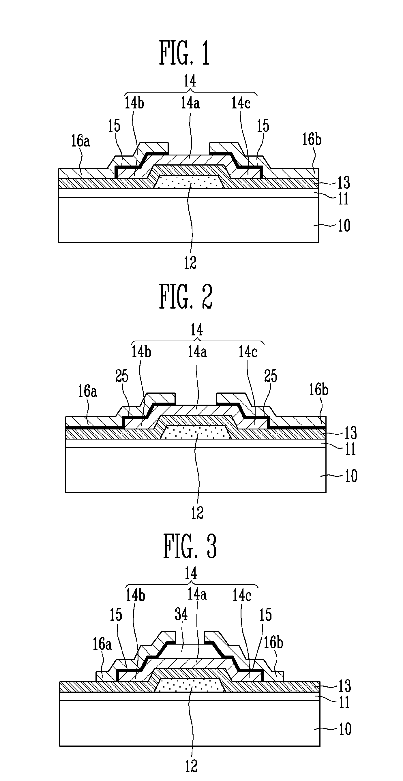
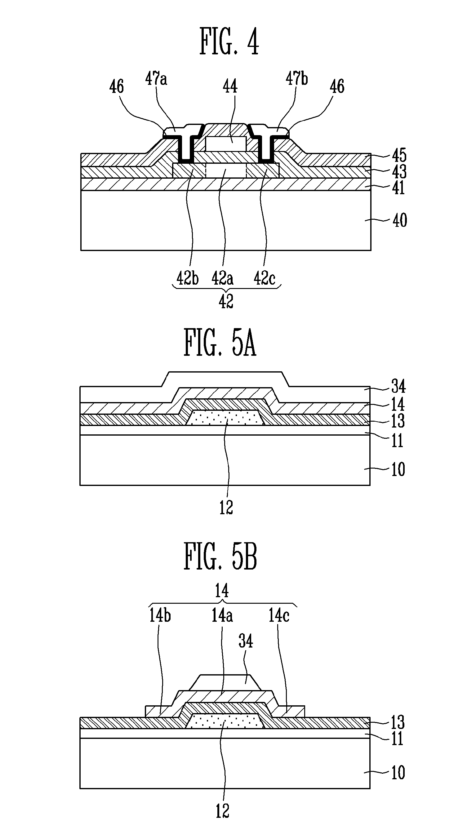
[0030]In the following detailed description, only certain exemplary embodiments of the present invention have been shown and described, simply by way of illustration. As those skilled in the art would realize, the described embodiments may be modified in various different ways, all without departing from the spirit or scope of the present invention. Accordingly, the drawings and description are to be regarded as illustrative in nature and not restrictive. In addition, when an element is referred to as being “on,”“formed on,” or “disposed on” another element, it can be directly on, formed directly on, or disposed directly on another element or one or more intervening elements may be disposed therebetween. Also, when an element is referred to as being “connected to,”“coupled to,” or “electrically coupled to” another element, it can be directly connected to another element or be indirectly connected to another element with one or more intervening elements interposed therebetween. Herei...


PUM


Abstract

A thin film transistor, a method of manufacturing the same, and a flat panel display device having the same use an oxide semiconductor as an active layer, wherein the thin film transistor includes: an oxide semiconductor layer formed on a substrate and having a channel region, a source region, and a drain region; a gate electrode insulated from the oxide semiconductor layer by a gate insulating layer; an ohmic contact layer formed on the source region and the drain region of the oxide semiconductor layer; and a source electrode and a drain electrode coupled to the source region and the drain region through the ohmic contact layer, the ohmic contact layer being formed of a metal having a lower work function lower than work functions of the source electrode and the drain electrode.

Description

CROSS-REFERENCE TO RELATED APPLICATIONS[0001]This application claims the benefit of Korean Patent Application No. 2008-57250, filed on Jun. 18, 2008, in the Korean Intellectual Property Office, the content of which is incorporated herein by reference.BACKGROUND OF THE INVENTION[0002]1. Field of the Invention[0003]Aspects of the present invention relate to a thin film transistor, a method of manufacturing the same, and a flat panel display device having the same, and particularly relates to a thin film transistor that uses an oxide semiconductor as an active layer, a method of manufacturing the same, and a flat panel display device having the same.[0004]2. Description of the Related Art[0005]Generally, in a thin film transistor manufactured by a semiconductor process, an active layer having a channel region, a source region, and a drain region is formed of a semiconductor, such as amorphous silicon or poly-silicon. However, if the active layer is formed of amorphous silicon, the acti...

Claims


Application Information

Patent Timeline
Patent Type & Authority Applications(United States)
IPC IPC(8): H01L29/786
CPCH01L29/7869H01L29/45
Inventor JEONG, JAE-KYEONGSHIN, HYUN-SOOMO, YEON-GON
Owner SAMSUNG DISPLAY CO LTD
Why Eureka
Try Eureka