Treated substrate having pattern of water repellent region, its production process, and process for producing member having pattern made of functional material film formed
a technology of functional material which is applied in the direction of photomechanical equipment, instruments, other chemical processes, etc., can solve the problems of inconvenience of device operation, low contrast between hydrophilic region and water repellent region in the pattern, etc., and achieve low amount of light, short time, and high contrast water repellent region
- Summary
- Abstract
- Description
- Claims
- Application Information
AI Technical Summary
Benefits of technology
Problems solved by technology
Method used
Image
Examples
example 1
Preparation of Treated Substrate 1
(Substrate Wash)
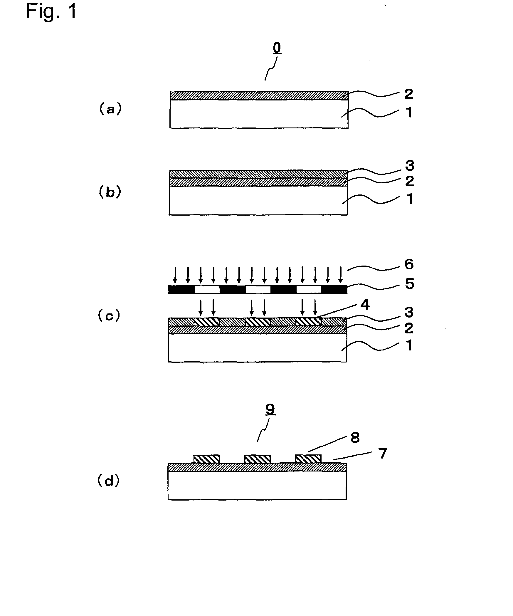
[0185]A 5 cm square silicon wafer was washed with ethanol and then subjected to UV / O3 washing.
(Coating with Solution)
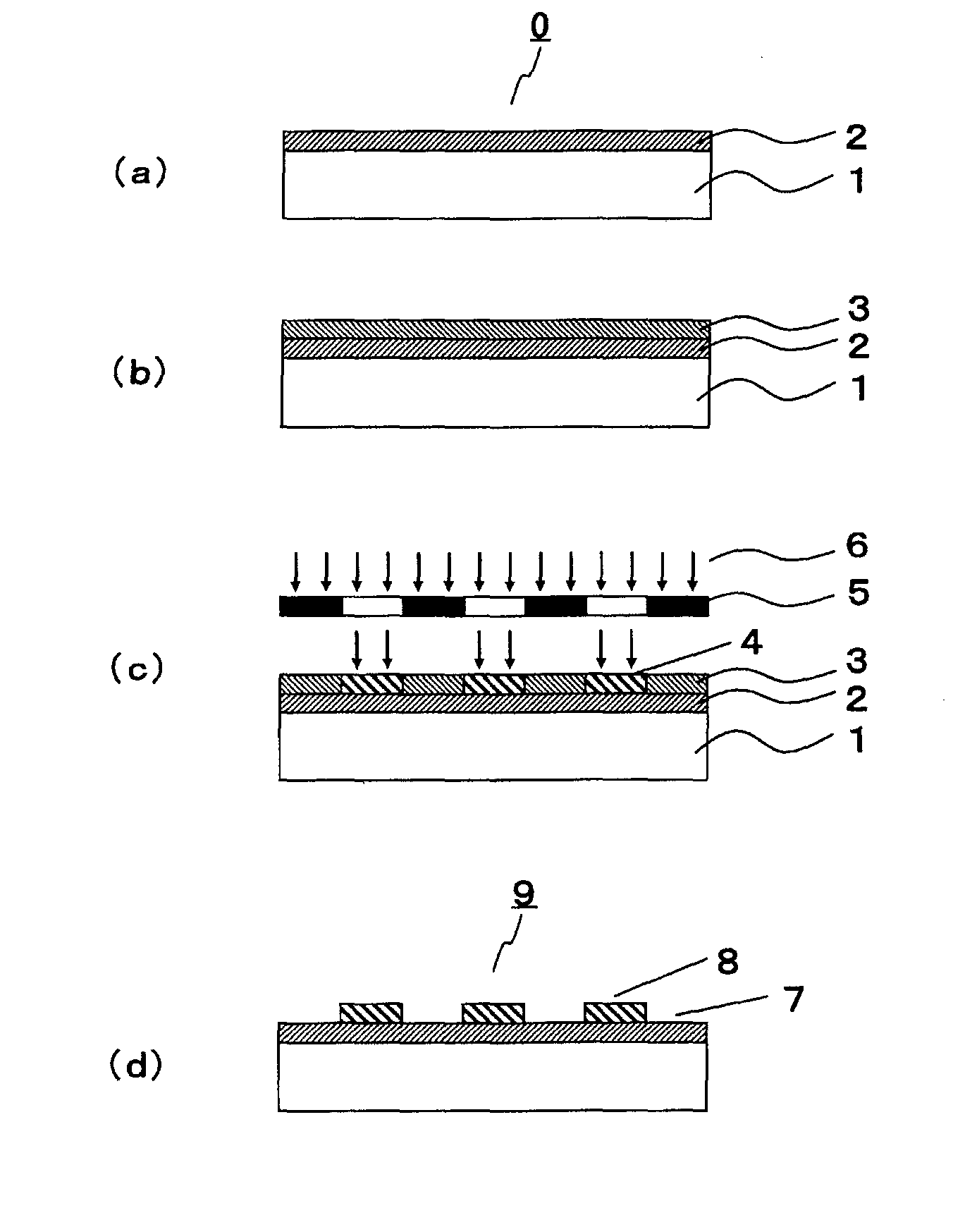
[0186]The silicon wafer was coated with the prepared solution (1) by spin coating (3,000 rpm, 20 seconds).
[0187]A surface of the obtained thin film was irradiated with ultraviolet light (wavelength: 300 to 450 nm) from an ultrahigh-pressure mercury lamp at 100 mw / cm2 for 30 seconds through a photomask having a pore pattern (2.5cm×5 cm).
(Substrate Wash)
[0188]The substrate was rinsed with isopropyl alcohol, then rinsed with ethanol and then dried in a nitrogen stream, whereby a treated substrate 1 was obtained.
example 2
Preparation of Treated Substrate 2
[0189]A treated substrate 2 was obtained in the same manner as in preparation of the treated substrate in Example 1 except that the solution (1) was changed to the solution (2), and the light irradiation conditions were changed at 100 mw / cm2 for 60 seconds.
example 3
Preparation of Treated Substrate 3
[0190]A treated substrate 3 was obtained in the same manner as in preparation of the treated substrate in Example 1 except that the solution (1) was changed to the solution (3), and the light irradiation conditions were changed at 100 mw / cm2 for 60 seconds.
PUM
| Property | Measurement | Unit |
|---|---|---|
| Thickness | aaaaa | aaaaa |
| Wavelength | aaaaa | aaaaa |
| Contact angle | aaaaa | aaaaa |
Abstract
Description
Claims
Application Information


