Semiconductor device

a technology of semiconductors and devices, applied in the direction of semiconductor devices, electrical equipment, transistors, etc., to achieve the effects of stable silicide layer, excellent high frequency characteristics, and stable base contact resistan

Inactive Publication Date: 2009-12-31
PANASONIC CORP
View PDF9 Cites 22 Cited by
  • Summary
  • Abstract
  • Description
  • Claims
  • Application Information

AI Technical Summary

Benefits of technology

[0034]As described above, the disclosed semiconductor device has the emitter layer of a double-layer structure. Therefore, the excellent high frequency chara

Problems solved by technology

However, the SiGe-HBT using the conventional non-selectiv

Method used


Image

  • Semiconductor device
  • Semiconductor device
  • Semiconductor device

Examples


first example embodiment

[0045]A first example embodiment of the present disclosure will be described with reference to the drawings.

[0046]A first example semiconductor device has a relatively thick Si-Cap layer constituting an intrinsic base layer; and an emitter layer formed in the intrinsic base layer which includes a lower emitter region having a deep junction formed by ion implantation, and an upper emitter region having a shallow junction formed by impurity diffusion (solid phase diffusion) from an emitter electrode.

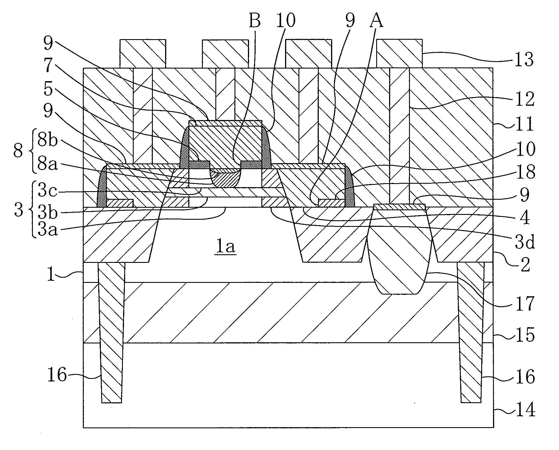
[0047]FIG. 1 shows the sectional structure of a SiGe heterojunction bipolar transistor (SiGe-HBT) as the first example semiconductor device.

[0048]As shown in FIG. 1, an N+-type impurity layer 15 which is a buried layer of about 500 nm in thickness formed on an upper portion of a P-type silicon (Si) semiconductor substrate 14. An N−-type epitaxial layer 1 of about 400 mn in thickness is formed on the N+-type impurity layer 15.

[0049]In the N−-type epitaxial layer, 1 first isolation regions (...

second example embodiment

[0084]A second example embodiment of the present invention will be described below with reference to the drawings.

[0085]A second example semiconductor device includes, in addition to the same double-layer emitter layer 8 as that of the first example semiconductor device, a retrograde collector region formed in part of the collector layer 1a below the emitter layer 8.

[0086]FIG. 6 shows the sectional structure of a SiGe heterojunction bipolar transistor (SiGe-HBT) as the second example semiconductor device. In FIG. 6, the same components as those shown in FIG. 1 are indicated by the same reference numerals to omit the explanation of them.

[0087]As shown in FIG. 6, the second example SiGe-HBT includes an N-type retrograde collector region 19 formed in part of the collector layer 1a below the emitter layer 8.

[0088]A method for manufacturing the retrograde collector region 19, which is a feature of the second example embodiment, will be explained below with reference to the drawings.

[0089...


PUM


Abstract

A semicoductor device includes: a collector layer made of a first conductivity type semiconductor; an intrinsic base layer formed on the collector layer and including a second conductivity type monocrystalline silicon germanium layer; a base extraction electrode formed around the intrinsic base layer and including a second conductivity type polycrystalline silicon layer and a second conductivity type polycrystalline silicon germanium layer; and a first conductivity type emitter layer formed in an upper portion of the intrinsic base layer. A silicon layer is formed in the upper portion of the intrinsic base layer and the emitter layer includes an upper emitter region formed in an upper portion of the silicon layer and a lower emitter region formed below and in contact with the upper emitter region.

Description

CROSS-REFERENCE TO RELATED APPLICATION[0001]This non-provisional application claims priority under 35 U.S.C. §119(a) of Japanese Patent Application No. 2008-168739 filed in Japan on Jun. 27, 2008, the entire contents of which are hereby incorporated by reference.BACKGROUND OF THE INVENTION[0002]The present disclosure relates generally to semiconductor devices, particularly to semiconductor devices having a silicon-germanium (SiGe) heterojunction with an epitaxially grown base layer.[0003]With the development of microprocessing and self-alignment technologies, improvement in capability of silicon bipolar transistors has been attempted. For higher performance, attention has been paid to an Epi-base structure including an epitaxially grown base layer.[0004]Particularly in recent years, researches and developments have been conducted actively on SiGe heterojunction bipolar transistors (SiGe-HBT) using an epitaxially grown SiGe mixed crystal semiconductor as a base layer. Above all, a no...

Claims


Application Information

Patent Timeline
IPC IPC(8): H01L29/72
CPCH01L29/1004H01L29/7371H01L29/66242
Inventor AOKI, SHIGETAKA
Owner PANASONIC CORP
Why Eureka
Try Eureka