Epitazial growth of crystalline material

a crystalline material and growth technology, applied in the growth process of polycrystalline materials, crystal growth processes, chemically reactive gases, etc., can solve the problems of unacceptably high dislocation density of epitaxially grown materials, unsatisfactory integration with silicon-based cmos technology, and inability to meet the requirements of a wide range of applications, so as to reduce surface roughness

Active Publication Date: 2009-12-31
TAIWAN SEMICON MFG CO LTD
View PDF10 Cites 89 Cited by
  • Summary
  • Abstract
  • Description
  • Claims
  • Application Information

AI Technical Summary

Benefits of technology

[0013]Therefore, it is an aspect of one embodiment of the invention to provid

Problems solved by technology

However, the dislocation density of the epitaxially grown material can be unacceptably high for many applications.
For example, the dislocation density of germanium directly grown on silicon can be as high as 108-109 cm−2 due to the 4.2% lattice mismatch between the two materials-unacceptable for most device applications.
However, these approaches may not be optimal for integration with silicon-based CMOS technology due to requirements for thick epi-layers and/or high thermal budgets, or due to incompatibility with selective growth at a density suitable for CMOS integration.
However, there are few studies on selective Ge, especially on the initial growth stage of Ge which determines the surface morphology of the layer.
Thus, the same devices produced on the same

Method used


Image

  • Epitazial growth of crystalline material
  • Epitazial growth of crystalline material
  • Epitazial growth of crystalline material

Examples


Embodiment Construction

[0027]Reference will now be made in detail to the embodiments of the present general inventive concept, examples of which are illustrated in the accompanying drawings, wherein like reference numerals refer to like elements throughout. The embodiments are described below in order to explain the present general inventive concept by referring to the figures.

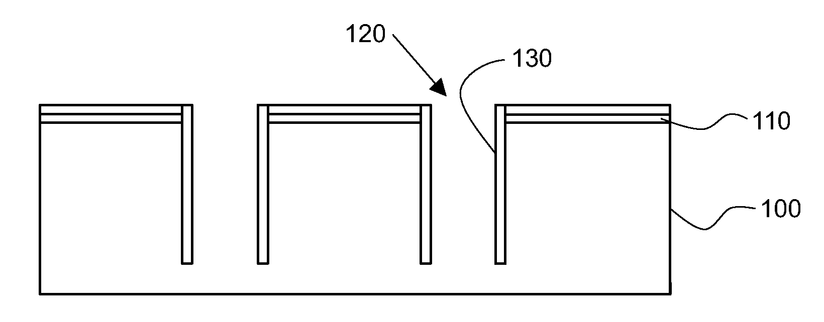
[0028]An embodiment of the invention is directed to a device including an epitaxially grown crystalline material in a opening in an insulator. FIG. 6A shows one example, illustrating a cross section of a portion of the device. As shown in FIG. 6A, the example includes a crystalline material 140 grown on a substrate 100 in a opening 120 defined in an insulator 110. The substrate 100 may be a crystalline material such as silicon, Ge or sapphire. Insulator 110 is preferably a non-crystalline material such as SiO2. The crystalline material at least at some stage in during its growth has a surface, for example surface 160, below the top ...


PUM


Abstract

A device includes an epitaxially grown crystalline material within an area confined by an insulator. A surface of the crystalline material has a reduced roughness. One example includes obtaining a surface with reduced roughness by creating process parameters which result in the dominant growth component of the crystal to be supplied laterally from side walls of the insulator. In a preferred embodiment, the area confined by the insulator is an opening in the insulator having an aspect ratio sufficient to trap defects using an ART technique.

Description

CROSS-REFERENCE TO RELATED APPLICATIONS[0001]The present application claims priority from U.S. provisional patent application, Ser. No. US61 / 058,542, filed Jun. 3, 2008, by Ji-Soo Park, incorporated by reference herein and for which benefit of the priority date is hereby claimed.BACKGROUND OF THE INVENTION[0002]1. Field of the Invention[0003]The present invention relates to epitaxial growth of a crystalline material. The improved growth may occur within a confined area, such as within a opening or trench formed in an insulator.[0004]2. Description of the Related Art[0005]The formation of lattice-mismatched materials has many practical applications. Heteroepitaxially growth of group IV materials or compounds, and III-V, III-N and II-VI compounds on a crystalline substrate, such as silicon has many applications such as photovoltaics, resonant tunneling diodes (RTD's), transistors (e.g., FET (which can be planar or 3D (i.e., finFET), HEMT, etc.), light-emitting diodes and laser diodes....

Claims


Application Information

Patent Timeline
IPC IPC(8): H01L29/20H01L21/20
CPCH01L21/0237H01L21/02521H01L21/02538H01L21/0262H01L21/02636H01L29/0684C30B25/186C30B29/08C30B29/40C30B29/403H01L21/02518C30B25/04H01L21/02381H01L21/02433H01L21/02532H01L29/165H01L29/34
Inventor PARK, JI-SOO
Owner TAIWAN SEMICON MFG CO LTD
Why Eureka
Try Eureka