Semiconductor device, production method thereof, and electronic device
a technology of semiconductor devices and production methods, applied in the direction of semiconductor devices, electrical devices, transistors, etc., can solve the problems of inaccurate determination of voltage or current the circuit needs, limited fet, etc., and achieve the effect of simple production steps, low resistance, and easy suppression of resistance variations among the tfts
- Summary
- Abstract
- Description
- Claims
- Application Information
AI Technical Summary
Benefits of technology
Problems solved by technology
Method used
Image

Examples
embodiment 1
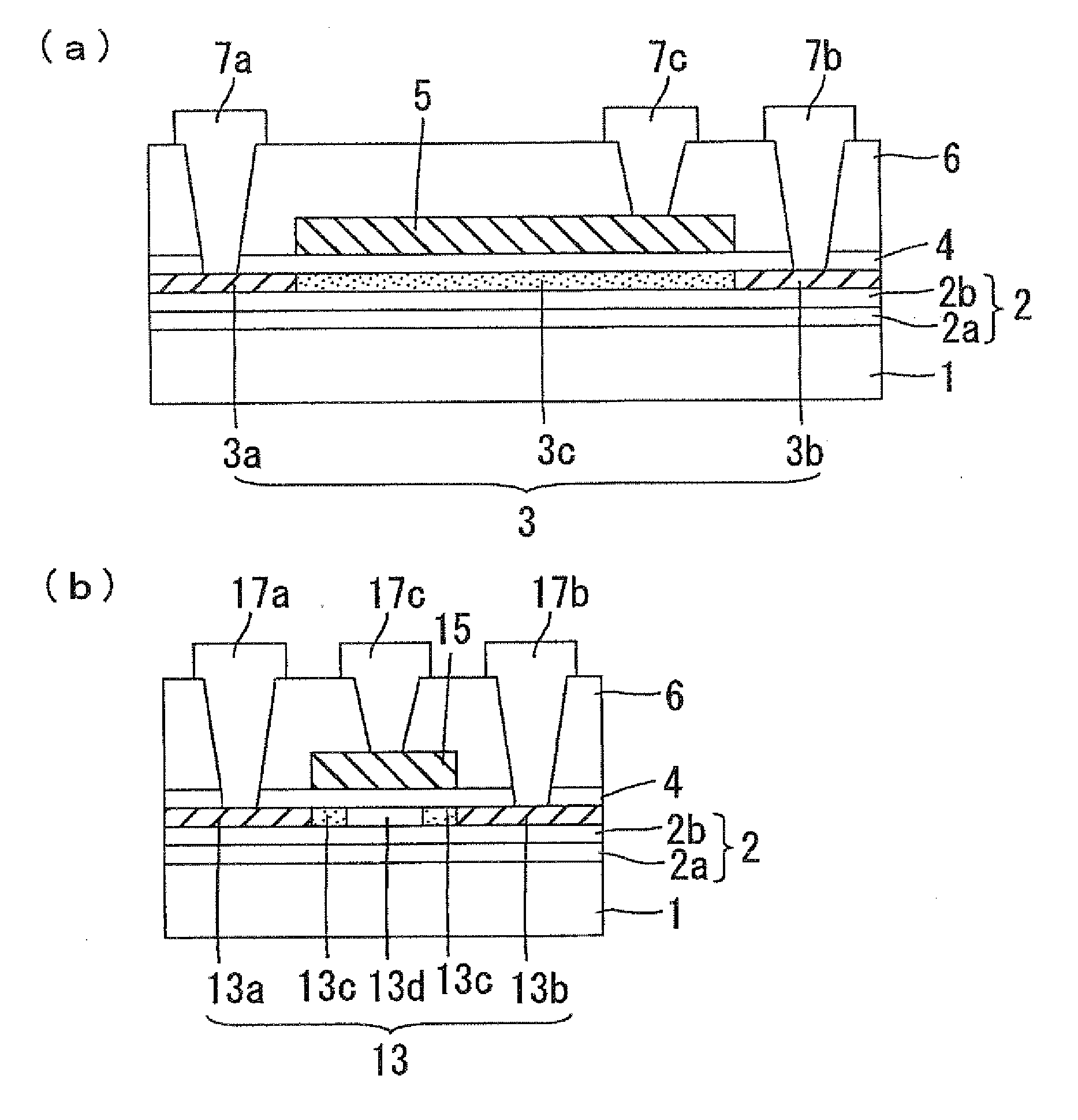
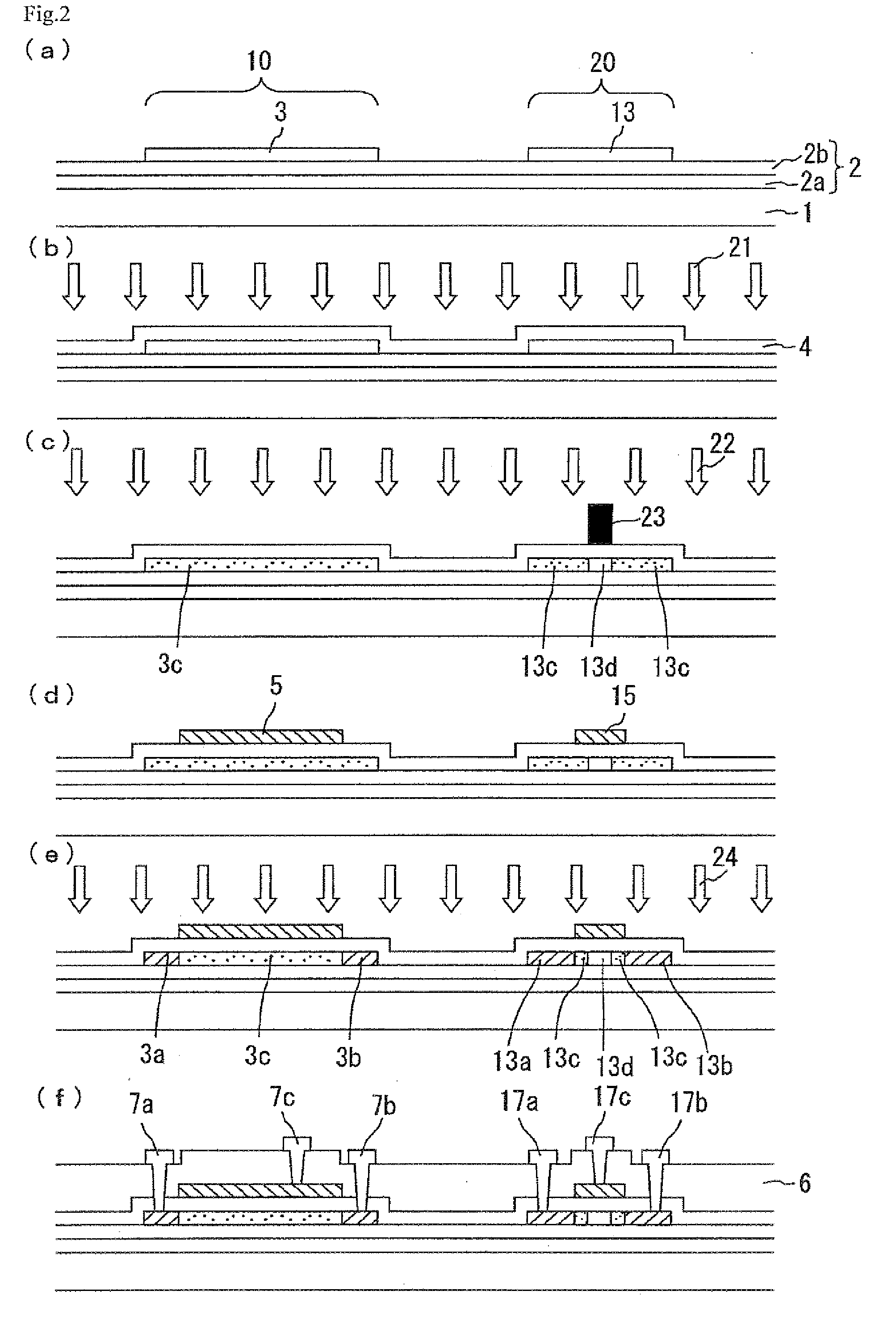
[0022]The configuration of the semiconductor device in Embodiment 1 of the present invention is mentioned below with reference to FIG. 1. FIG. 1(a) is a cross sectional view schematically showing the first TFT which is used as a resistance element (hereinafter, also referred to as a resistance element TFT) of the semiconductor device in Embodiment 1. FIG. 1(b) is a cross sectional view schematically showing the second TFT having a GOLD structure which is used as a driving control element (hereinafter, also referred to as a COLD structure TFT) of the semiconductor device in Embodiment 1. According to the semiconductor device in the present Embodiment, the resistance element TFT and the GOLD structure TFT are formed on the same substrate.
[0023]As shown in FIG. 1(a), according to the configuration of the resistance element TFT used in Embodiment 1, the first insulating film 2 composed of an impurity diffusion barrier film 2a and a stress relaxation layer 2b is formed on a substrate 1. ...
PUM
 Abstract
Description
Claims
Application Information
 - R&D
- Intellectual Property
- Life Sciences
- Materials
- Tech Scout
- Unparalleled Data Quality
- Higher Quality Content
- 60% Fewer Hallucinations
Browse by: Latest US Patents, China's latest patents, Technical Efficacy Thesaurus, Application Domain, Technology Topic, Popular Technical Reports.
© 2025 PatSnap. All rights reserved.Legal|Privacy policy|Modern Slavery Act Transparency Statement|Sitemap|About US| Contact US: help@patsnap.com