Manufacturing method of strained si substrate

a technology manufacturing method, which is applied in the direction of polycrystalline material growth, chemically reactive gas growth, crystal growth process, etc., can solve the problems of increasing the density of threading dislocation, deteriorating surface roughness, and not obtaining a sufficient high quality of strained si substrate, etc., to achieve low threading dislocation density, high quality, and high quality

Inactive Publication Date: 2010-01-07
SHIN-ETSU HANDOTAI CO LTD
View PDF6 Cites 109 Cited by
  • Summary
  • Abstract
  • Description
  • Claims
  • Application Information

AI Technical Summary

Benefits of technology

[0011]The present invention has been made in view of the above-mentioned circumstances, and an object of the present invention is to provide a manufacturing method of a strained Si substrate having low surface roughness, threading dislocation density and particle level.

Problems solved by technology

In the strained Si substrate, however, since dislocation is generated on the SiGe layer due to the difference in lattice constant between the Si substrate and the SiGe layer to be deposited on its surface, irregularities (cross-hatching patterns) are caused on the surface of the SiGe layer, so that a strained Si substrate with a sufficient high quality has not been obtained yet.
However, in both of the methods disclosed in the publication of Unexamined Japanese Patent Application No. 2000-513507 and in the publication of Unexamined Japanese Patent Application No. 2002-289533, deterioration of the surface roughness and the increase in the threading dislocation density are induced during epitaxial growth (hereinafter referred to as epi-growth) of the strained Si on the SiGe layer surface, specifically in the heat-treatment processes both in removing native oxide film and in epi-growth of the strained Si, so that the methods are insufficient for obtaining a high-quality strained Si substrate.
Since the step of removing the native oxide film on the SiGe layer surface especially requires the highest temperature during the epi-growth of the strained Si, how to lower the temperature in the process is a key issue.
The process including HF cleaning at the last step, however, has a fundamental problem that particles tend to be attached, so that a strained Si substrate having a poor particle level is generated.
However, with the method disclosed in the above-mentioned publication of Unexamined Japanese Patent Application No. 2001-148473, the particles attached on the surface are not removed enough, and the above-mentioned Publication of Unexamined Japanese Patent Application No. 2003-31495 does not mention a cleaning step at all.
Therefore, it is difficult with both of the two methods to obtain a strained Si substrate having a sufficient surface roughness and a low particle level.

Method used


Image

  • Manufacturing method of strained si substrate
  • Manufacturing method of strained si substrate
  • Manufacturing method of strained si substrate

Examples


experimental example 1

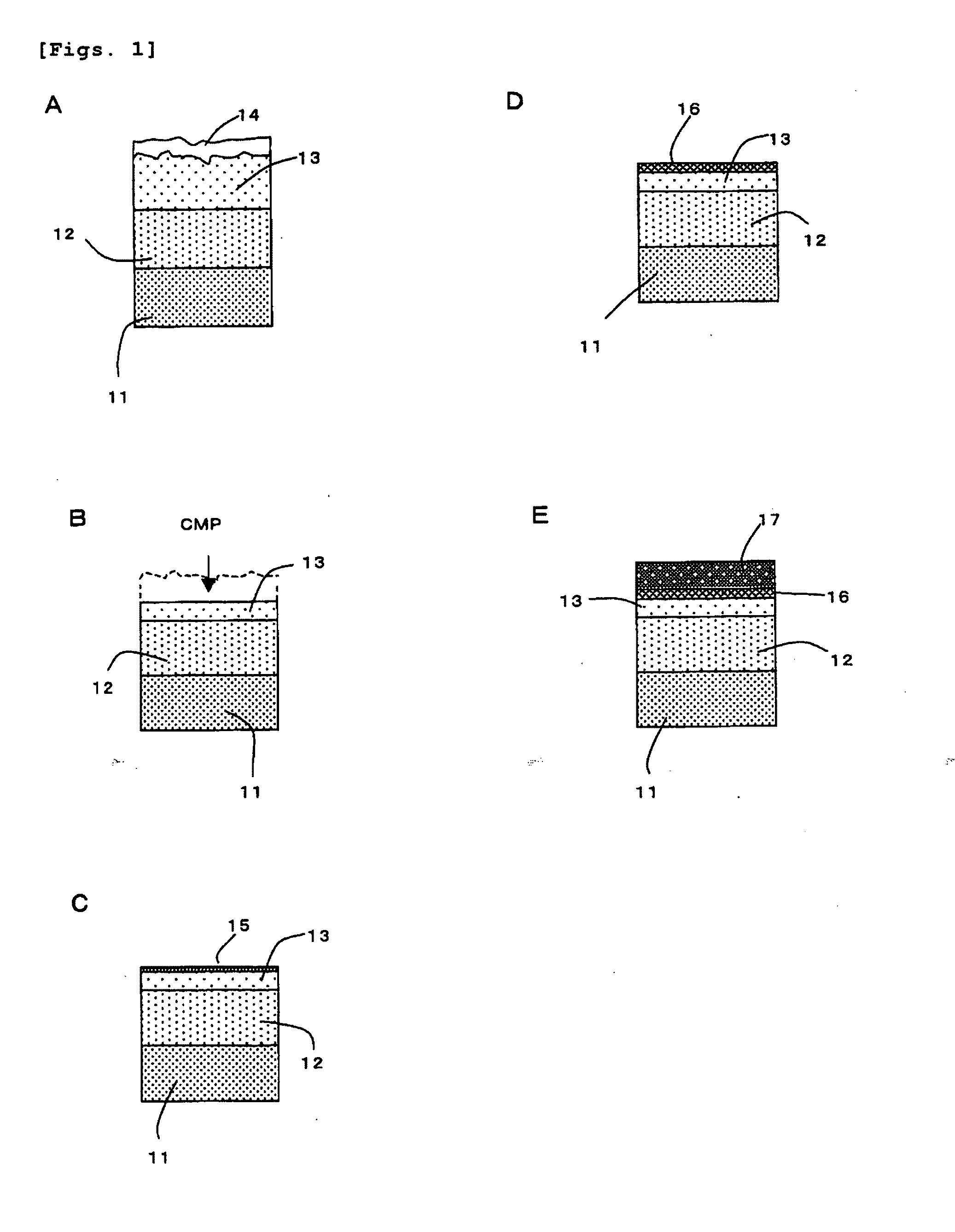
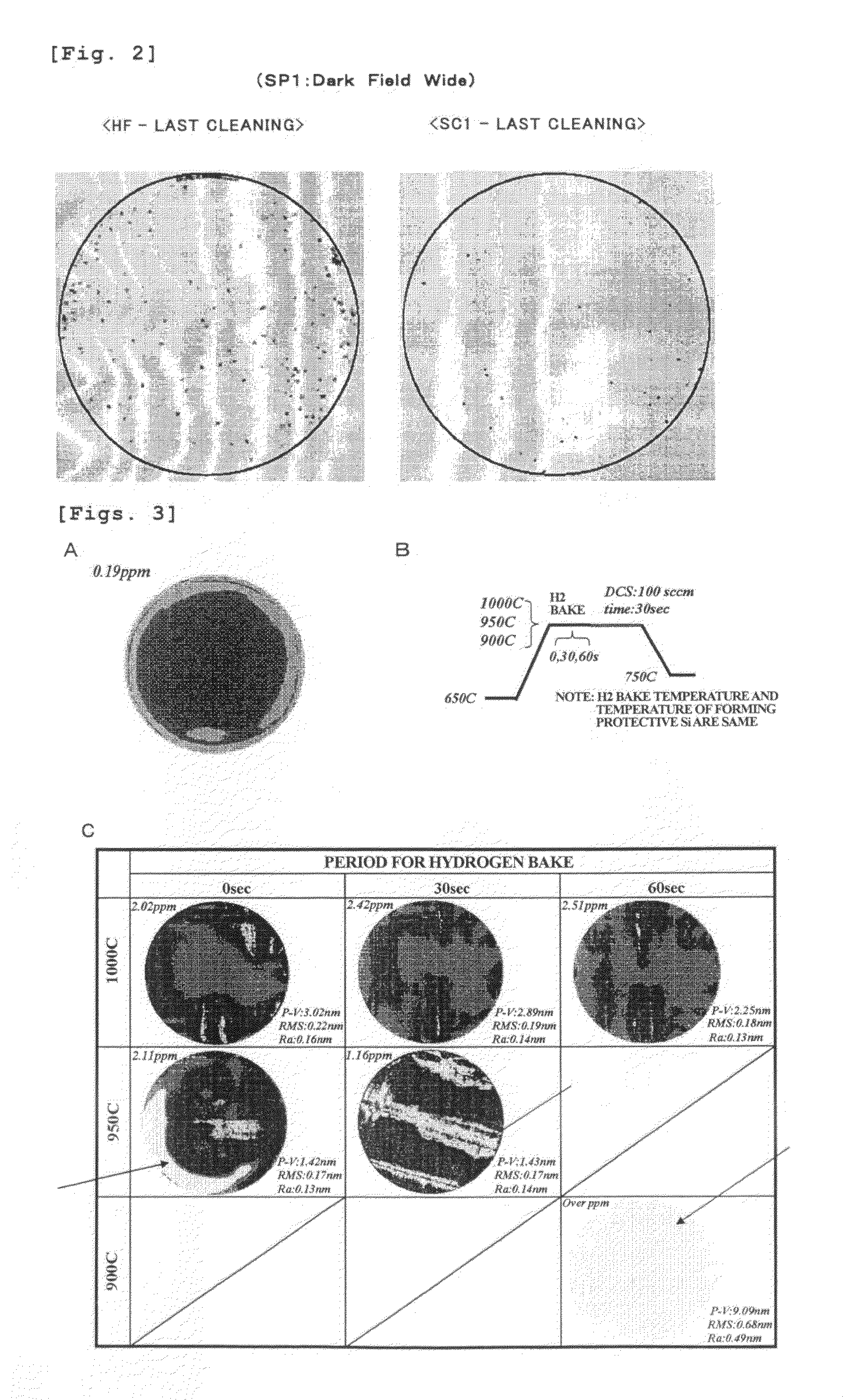
[0062]As the last cleaning step of a wafer surface for the semiconductor substrate after the CMP, HF finishing and SC1 finishing were compared (See FIG. 2).

1) The above-mentioned semiconductor substrate was subjected to SC1 cleaning in a mixed liquid of NH4OH:H2O2:H2O=1:1:5, DHF (5%) cleaning, and spin-drying at 76° C., and then was measured with respect to its particle level on the wafer surface by a particle measuring instrument (SP1, manufactured by KLA-Tencor Corporation) in a Dark Field Wide mode (See FIG. 2, left-hand side).

2) The above-mentioned semiconductor substrate was subjected to SC1 cleaning in a mixed liquid of NH4OH:H2O2:H2O=1:1:5, and spin-drying at 76° C., and then was measured with respect to its particle level on the wafer surface by a particle measuring instrument (SP1) in a Dark Field Wide mode (See FIG. 2, right-hand side).

[0063]As is also apparent from FIG. 2, when the wafer cleaning was finished with HF, particles were very easy to be attached.

experimental example 2

[0064]With respect to the semiconductor substrate which was subjected to the above-mentioned CMP and to SC1-cleaning under conditions of the above-mentioned Experimental Example 1 as the last cleaning process of the wafer (as shown in FIG. 1C), H2 bake was performed using a CVD device of single wafer processing type for the purpose of removing native oxide film 15 formed in the SC1 cleaning, under a reduced pressure at each of the below-mentioned temperatures for each of the below-mentioned time periods so as to examine the optimal conditions.

[0065]Under a reduced pressure of 80 torr (about 11 kPa), the H2 bake temperature was raised from 650° C. to 900° C., 950° C. and 1000° C., respectively, and for each temperature case, H2 bake processing was performed for a constant time period (0 second, 30 seconds and 60 seconds), respectively, and then the reaction using DCS (100 sccm) was performed at the same temperature as that for the H2 bake for 30 seconds so as to form a protective Si ...

examples 1 and 2

, and Comparative Examples 1 and 2

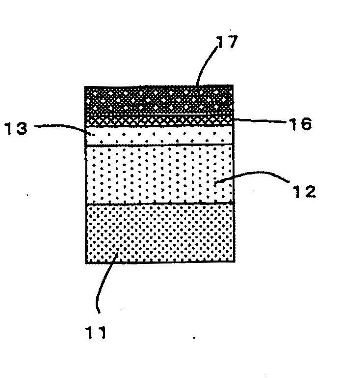
[0073]In Examples 1 and 2 shown in FIG. 4C, immediately after H2 bake, a protective Si layer 16 was formed with a thickness of 5 nm, then the temperature was lowered to 800° C. or 650° C. which was a temperature for growing a strained Si, and then a strained Si layer 17 was epitaxially grown with a thickness of 70 nm. In Comparative Examples 1 and 2, after H2 bake, still in H2 atmosphere, the temperature was lowered to 800° C. or 650° C. which was a temperature for growing a strained Si, and then a strained Si layer 17 was epitaxially grown with the thickness of 70 nm. Haze level under each condition was measured.

[0074]As a reference, FIG. 4A shows a haze level on a wafer surface before H2 bake (0.19 ppm). FIG. 4B shows recipe of the above-mentioned reaction, and it shows specifically that a wafer was inserted into a CVD device at 650° C., that temperature was raised to 1000° C. in a hydrogen atmosphere, that immediately DCS was flowed for three sec...


PUM

PropertyMeasurementUnit
temperatureaaaaaaaaaa
thicknessaaaaaaaaaa
surface roughnessaaaaaaaaaa

Abstract

According to the present invention, there is provided a manufacturing method of a strained Si substrate including at least steps of: forming a lattice-relaxed SiGe layer on a silicon single crystal substrate; flattening a surface of the SiGe layer by CMP; and forming a strained Si layer on the surface of the flattened SiGe layer, wherein the method comprises steps of: subjecting the surface of the SiGe layer to SC1 cleaning, before forming the strained Si layer on the lattice-relaxed SiGe layer surface that is flattened; heat-treating the substrate having the SiGe layer after being subjected to SC1 cleaning in a hydrogen-containing atmosphere at 800° C. or higher; immediately forming a protective Si layer on the SiGe layer surface on the heat-treated substrate, without lowering the temperature below 800° C. after the heat treatment; and forming the strained Si layer on the surface of the protective Si layer at a temperature lower than the temperature of forming the protective Si layer. Thereby, a manufacturing method of a strained Si substrate having low surface roughness, threading dislocation density and low particle level can be provided.

Description

TECHNICAL FIELD[0001]The present invention relates to a manufacturing method of a strained Si substrate of a bulk type or SOI type used for a high-speed MOSFET.BACKGROUND ART[0002]In a strained Si substrate of a bulk type where a SiGe layer with graded concentration having an increased Ge concentration with increased thickness is formed on a Si substrate, a SiGe layer with constant concentration having a constant Ge concentration is formed thereon, and a Si layer is further formed thereon, since the Si layer is formed on the SiGe layer having a greater lattice constant than that of Si, the lattice constant of the Si layer is extended (tensile strain is caused), so that strain is generated. It is known that when the lattice constant of the Si layer in the device forming area is thus extended, mobility of electrons and holes is improved, which contributes to achieving high-performance of MOSFET (Metal Oxide Semiconductor Field Effect Transistor).[0003]In the strained Si substrate, how...

Claims


Application Information

Patent Timeline
Patent Type & Authority Applications(United States)
IPC IPC(8): H01L21/762H01L21/20
CPCC30B25/183C30B29/06H01L21/02381H01L21/02661H01L21/0251H01L21/02532H01L21/0262H01L21/0245H01L21/20H01L27/12
Inventor OKA, SATOSHINOTO, NOBUHIKO
Owner SHIN-ETSU HANDOTAI CO LTD
Why Eureka
Try Eureka