Fault detection and classification method for wafer acceptance test parameters
- Summary
- Abstract
- Description
- Claims
- Application Information
AI Technical Summary
Benefits of technology
Problems solved by technology
Method used
Image

Examples
first embodiment
The First Embodiment
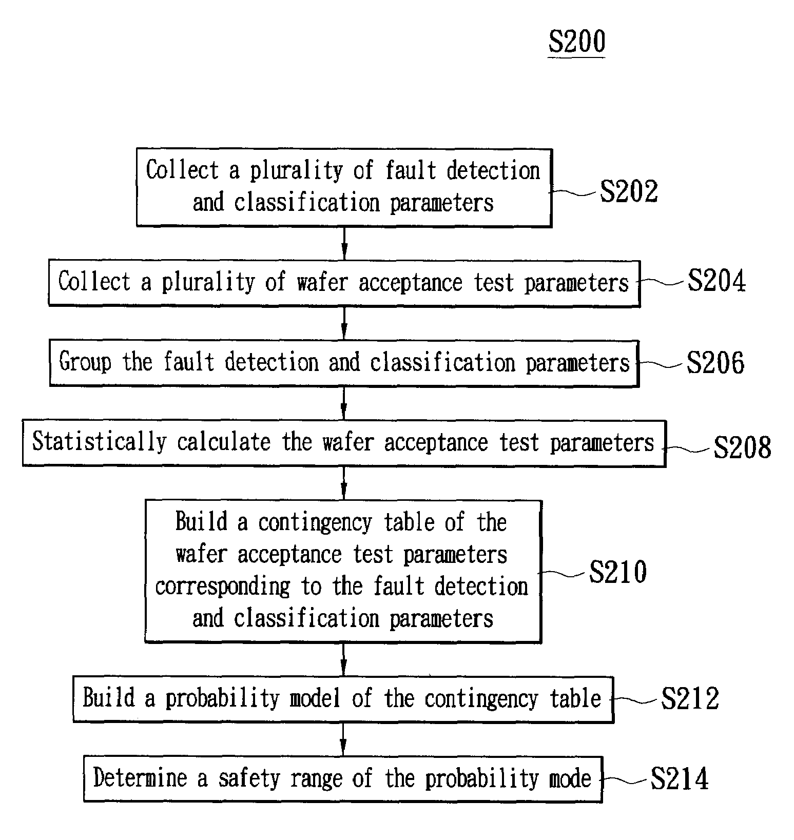
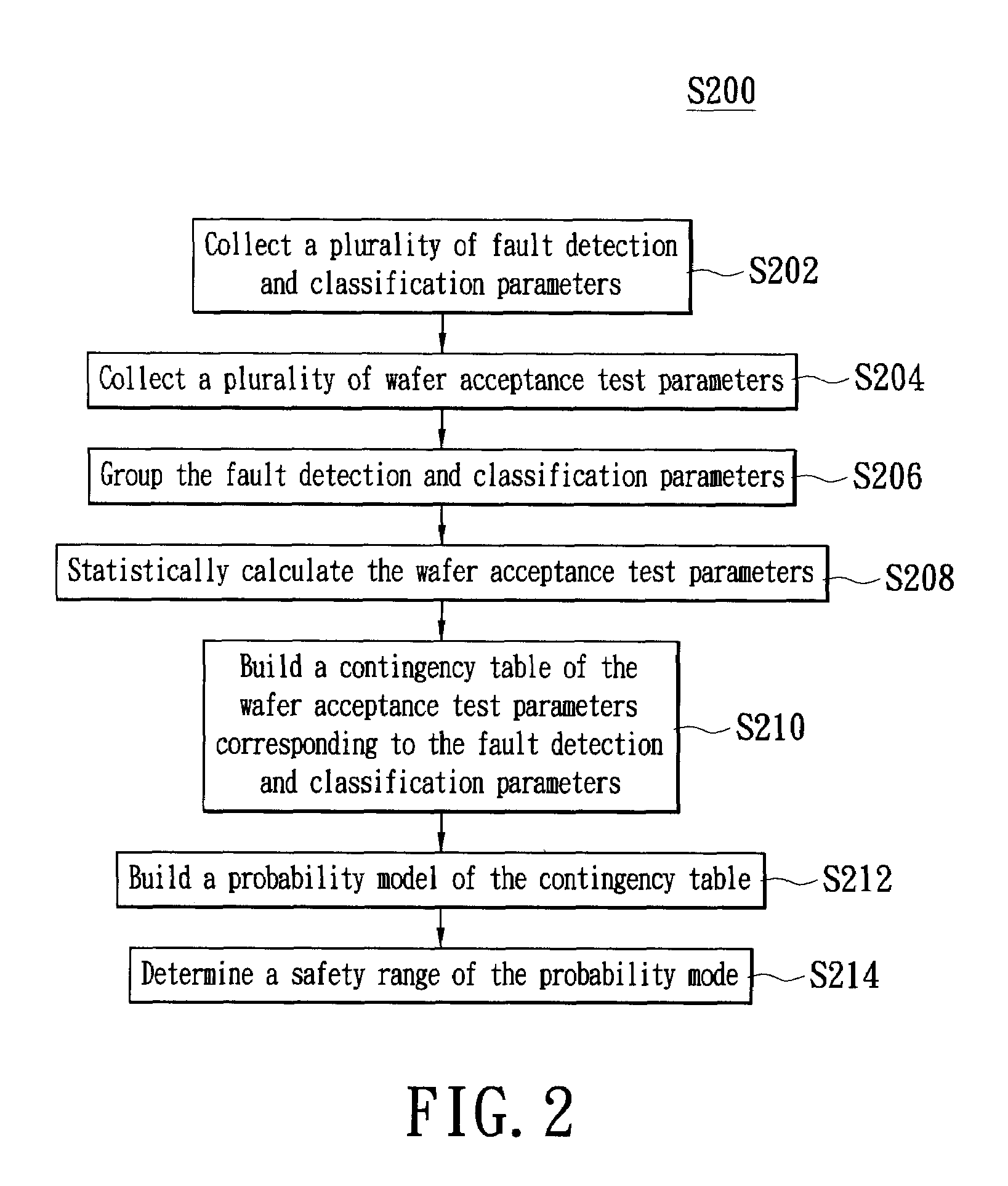
[0026]Reference is made to FIG. 2, which shows the fault detection and classification (FDC) method S200 for wafer acceptance test (WAT) parameters of the first embodiment of the present invention. The method includes the following steps.
[0027]Step S202 is performed. Reference is made to FIG. 3. A plurality of fault detection and classification parameters 302 is collected. For example, the fault detection and classification parameters 302 are the plurality of manufacturing process parameters of a semiconductor manufacturing process machine.
[0028]Step S204 is performed. A plurality of wafer acceptance test parameters 304 that is corresponded by the fault detection and classification parameters 302 is collected. In this embodiment, the plurality of wafer acceptance test parameters 304 includes a plurality of first wafer acceptance test parameters 304a, a plurality of second wafer acceptance test parameters 304b, and a plurality of third wafer acceptance test paramet...
second embodiment
The Second Embodiment
[0045]Reference is made to FIG. 7, which shows the fault detection and classification method S700 for wafer acceptance test parameters of the second embodiment of the present invention. The method includes the following steps.
[0046]Step S702 is performed. A contingency table (not shown in the figure) is built. The contingency table has a plurality of wafer acceptance test parameters (not shown in the figure) and a plurality of fault detection and classification parameters (not shown in the figure).
[0047]In this embodiment, referring to FIGS. 8A˜8I, which show the curved diagrams of the data distribution of the wafer acceptance test parameters corresponding to the fault detection and classification parameters. The flowing steps are also included. The fault detection and classification parameters are collected, the wafer acceptance test parameters corresponded by the fault detection and classification parameters are collected, and the fault detection and classific...
PUM
 Abstract
Description
Claims
Application Information