Apparatus for high-rate chemical vapor deposition

Inactive Publication Date: 2010-01-21
CHEN YUNG TIN
View PDF8 Cites 14 Cited by
  • Summary
  • Abstract
  • Description
  • Claims
  • Application Information

AI Technical Summary

Benefits of technology

[0022]According to the present invention, the film forming gas in the chamber is excited and decomposed by the laser sheet, which passes between the discharge electrode and the substrate in parallel with the substrate along a plane spaced apart therefrom, and concurrent ionization

Problems solved by technology

While a-Si:H based solar cells and TFT devices have been commercially produced by PECVD for years, the production of thicker nc-Si:H films by PECVD is limited by the deposition rate thereof.
As the film forming rate of nc-Si:H is increased by increasing the RF power input, however, the bombardment of the growing nc-Si:H film on the substrate by highly energized ions also increases, thereby generating film structural defects that have deleterious effects on electrical properties thereof.
However, there are several drawbacks in applying the conventional laser beam CVD process in production of solar cells and TFT devices, which requires dense and uniform semiconductor films deposited over large area substrates.
A problem associated with the conventional laser CVD process described above is that since the reaction product reaches the substrate surface by diffusing away from the laser effected zone, which is defined by the narrow path of the laser beam above the substrate, the concentration of the reaction product on the substrate surface will depend on the distance away from the path of the laser beam, thereby causing the film thickness on the substrate to vary in the direction perpendicular to the path of the laser beam.
While it is possible to improve the film uniformity on the substrate by increasing the distance between the beam path and the substrate surface, doing so will adversely decrease the film deposition rate.
Another problem associated with the conventional l

Method used


Image

  • Apparatus for high-rate chemical vapor deposition
  • Apparatus for high-rate chemical vapor deposition
  • Apparatus for high-rate chemical vapor deposition

Examples


first embodiment

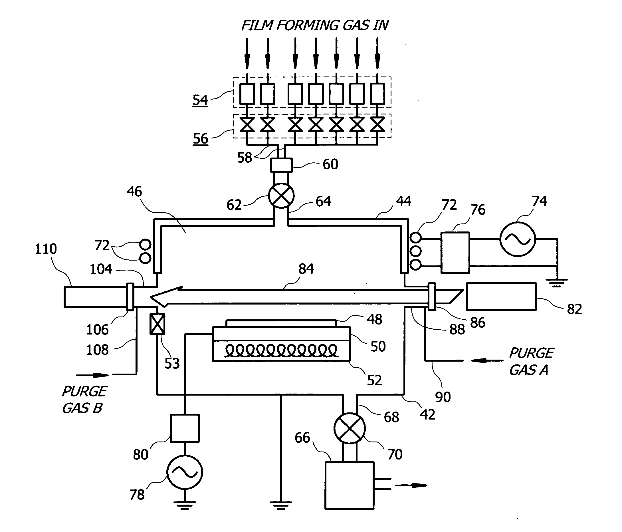
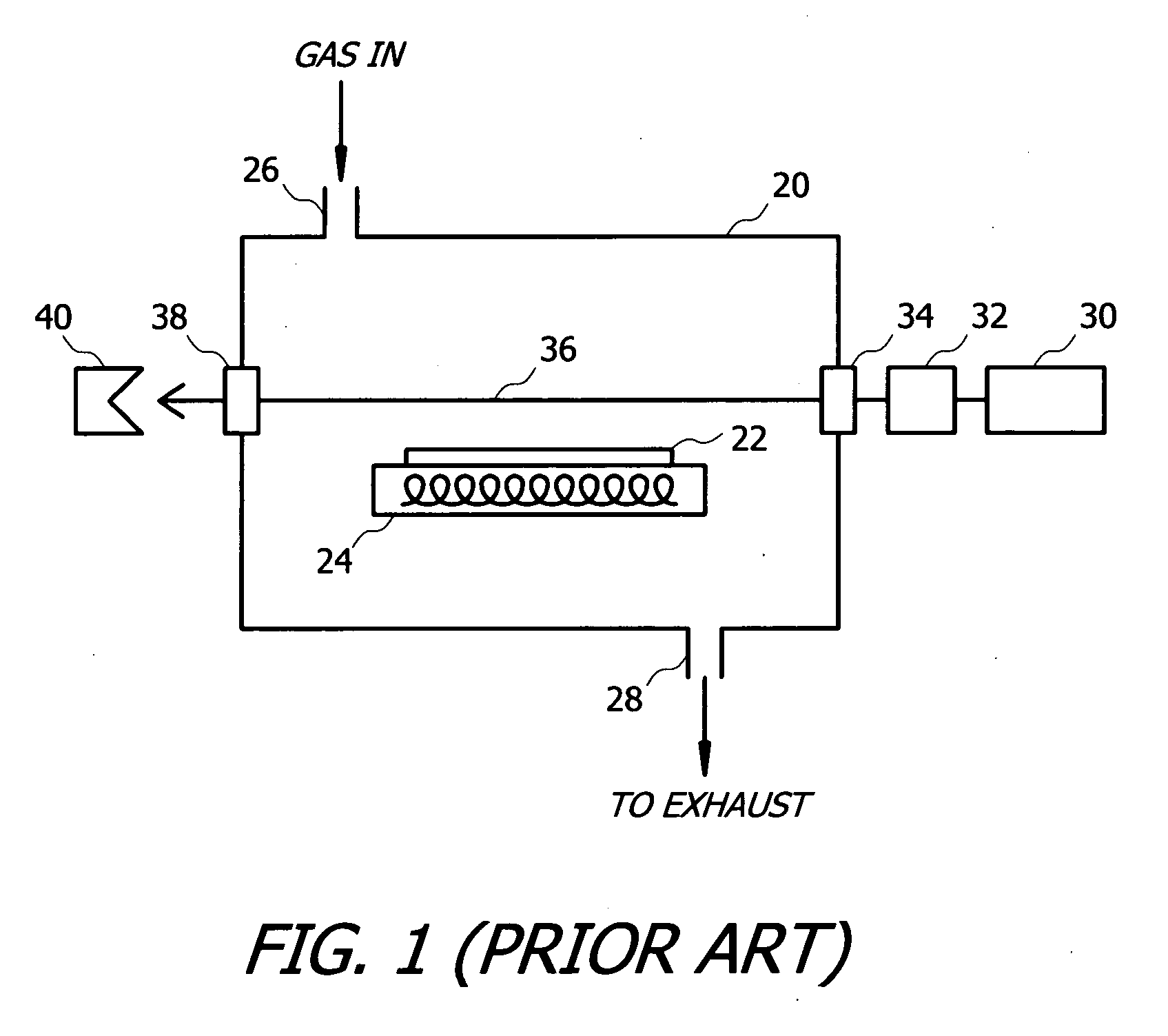
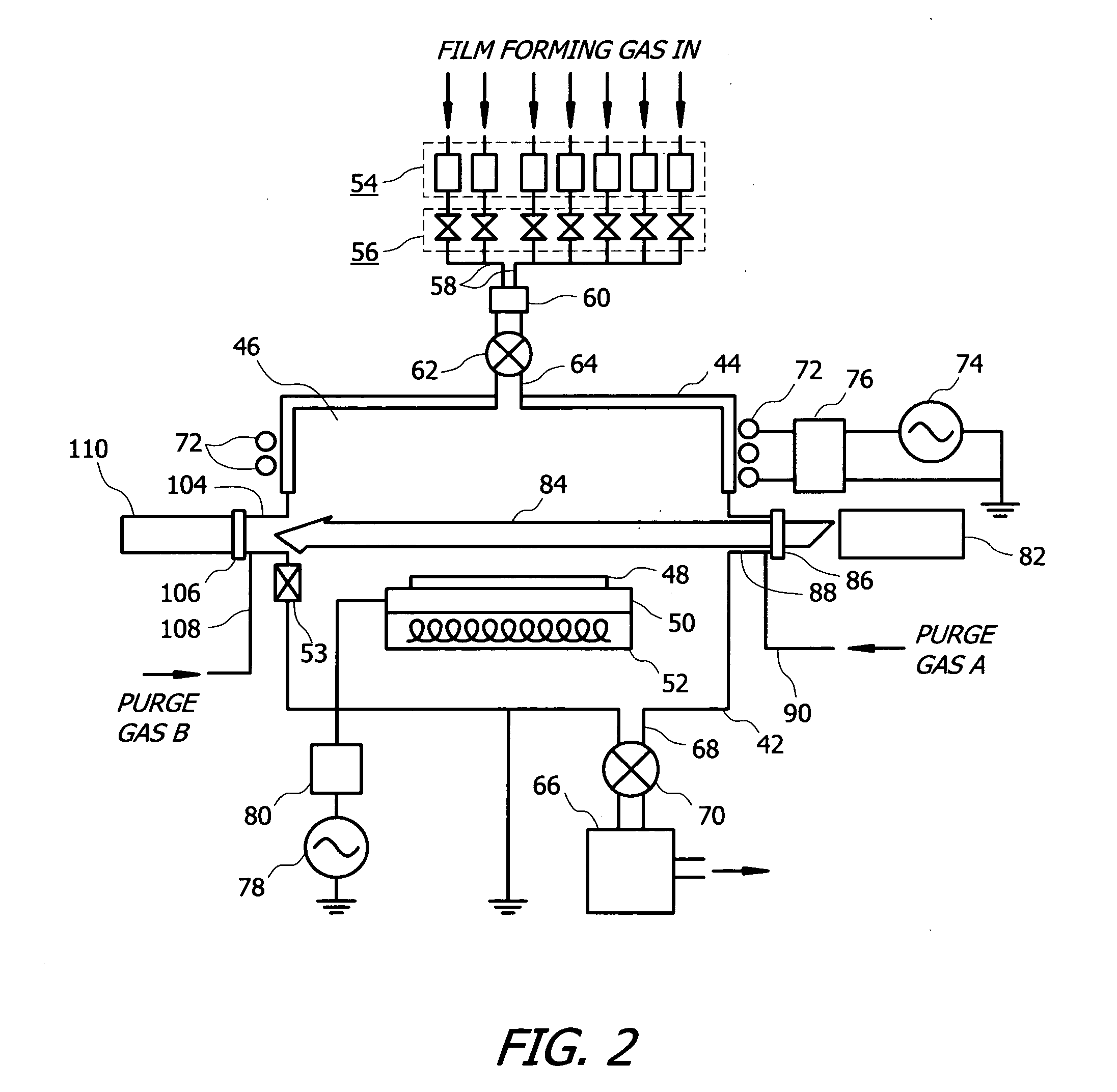
[0032]the present invention as applied to a high-rate chemical vapor deposition (CVD) apparatus for forming semiconductor thin films will now be described with reference to FIG. 2. Referring now to FIG. 2, the illustrated apparatus has a vessel base 42, preferably constructed of a suitably strong and conductive material such as stainless steel and is electrically grounded, and a vessel top or dome 44, which is made of a dielectric material such as aluminum oxide or aluminum nitride. The base 42 and the dome 44 combined to define a reaction chamber 46 therein.

[0033]A generally flat substrate 48 for coating a film thereon is placed inside the reaction chamber 46. The substrate 48 is supported by a mounting base 50, which also serves as a bias electrode. A suceptor 52 for heating the substrate 48 is attached to the bottom surface of the mounting base 50, and incorporates therein a heating element which may be energized from a current source (not shown) external to the chamber 46. The s...

fourth embodiment

[0048]FIG. 6 shows a high-rate CVD apparatus in accordance with the present invention. The illustrated apparatus has a reaction vessel 128 which defines a reaction chamber 130 therein. A generally flat substrate 132 for coating a film thereon is placed inside the reaction chamber 130. The substrate 132 is supported by a mounting base 134, preferably made of an electrically conducting metal. A suceptor 136 for heating the substrate 132 is attached to the bottom surface of the mounting base 134, and incorporates therein a heating element which may be energized from a current source (not shown) external to the chamber 130. The substrate 132 is transported in and out of the chamber 130 through a shutter 138 disposed on the sidewall of the vessel 128.

[0049]Gases from a plurality of external gas sources for forming semiconductor films, such as SiH4, GeH4, CH4, C3H8, H2, B2H6 and PH3, are controlled by a set of corresponding MFCs 140 and control valves 142, and pass through gas delivery li...


PUM

PropertyMeasurementUnit
Transparencyaaaaaaaaaa
Frequencyaaaaaaaaaa

Abstract

An apparatus for high-rate chemical vapor (CVD) deposition of semiconductor films comprises a reaction chamber for receiving therein a substrate and a film forming gas, a gas inlet for introducing the film forming gas into the reaction chamber, an incidence window in the reaction chamber for transmission of a laser sheet into the reaction chamber, a laser disposed outside the reaction chamber for generating the laser sheet and an antenna disposed outside the reaction chamber for generating a plasma therein. The film forming gas in the chamber is excited and decomposed by the laser sheet, which passes in parallel with the substrate along a plane spaced apart therefrom, and concurrent ionization effected by the antenna, thereby forming a dense semiconductor film on the substrate at high rate.

Description

RELATED APPLICATIONS[0001]The present application is a continuation-in-part application of U.S. provisional patent application, Ser. No. 61 / 135,240, filed Jul. 19, 2008, for APPARATUS FOR HIGH-RATE CHEMICAL VAPOR DEPOSITION, by Yung-Tin Chen, included by reference herein and for which benefit of the priority date is hereby claimed.BACKGROUND [0002]1. Field of Invention[0003]The present invention relates to an apparatus for depositing semiconductor films, and more particularly to a chemical vapor deposition (CVD) apparatus utilizing plasma and laser excitation means for high-throughput manufacturing of solar cells and thin-film transistor (TFT) devices.[0004]2. Description of Prior Art[0005]Hydrogenated amorphous silicon (a-Si:H) and nano-crystalline silicon (nc-Si:H) are widely used in thin film solar cells because they can be fabricated over large area substrates as required by photovoltaic applications. Compared with amorphous Si, nc-Si:H may produce solar cells with higher effici...

Claims


Application Information

Patent Timeline
IPC IPC(8): C23C16/448
CPCC23C16/505C23C16/483
Inventor CHEN, YUNG-TIN
Owner CHEN YUNG TIN
Why Eureka
Try Eureka