
Eureka
For R&D, Eureka makes reading and utilizing patents & technical documents easy.
Eureka AIR
Designed for self-driven R&D workflows. Generate viable solutions, solve complex R&D challenges, empower your innovation with AI.

Eureka Materials
Designed for material experts only. Revolutionize your material R&D, from search, analyze, to developing new materials.

TechResearch
Generate reliable direction feasibility study reports for your R&D in just a few steps.

TechSeek
Discover and master advanced knowledge NOW. Basics, ideas, possibilities, all at once.

TechMind
As an expert in R&D Theories, TechMind can generates customized viable solutions instantly.

TechRisk
Analyze your overall solution with one click, know your potential R&D risks in advance.

TechMonitor
Get weekly tech updates, stay abreast of the latest tech innovations and key insights.
Method for manufacturing iii-v compound semiconductor substrate, method for manufacturing epitaxial wafer, iii-v compound semiconductor substrate, and epitaxial wafer
- Summary
- Abstract
- Description
- Claims
- Application Information
AI Technical Summary
Benefits of technology
Problems solved by technology
Method used
Image

Examples
first embodiment
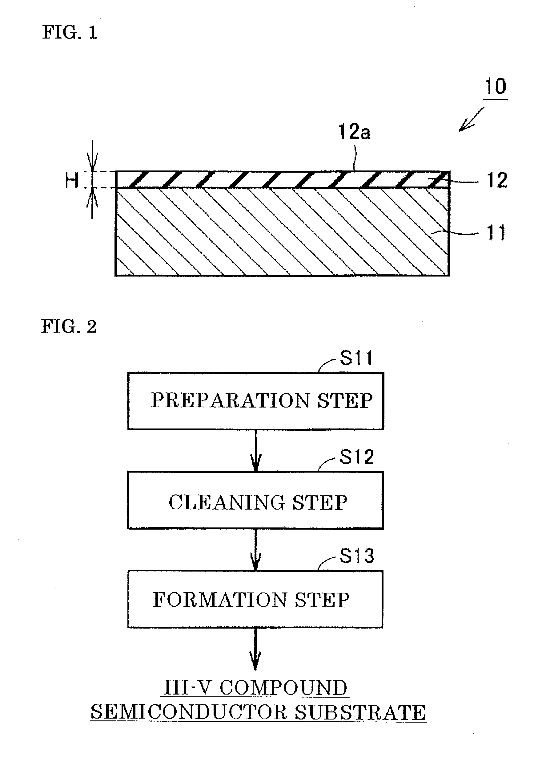
[0046]FIG. 1 is a sectional view schematically showing a III-V compound semiconductor substrate according to the present embodiment. The III-V compound semiconductor substrate according to the present embodiment will be described with reference to FIG. 1.
[0047]As shown in FIG. 1, a III-V compound semiconductor substrate 10 according to the present embodiment includes a substrate 11 and an oxide film 12. The oxide film 12 is disposed on the substrate 11.
[0048]The substrate 11 is composed of a III-V compound semiconductor containing GaAs, InP, GaN, aluminum nitride (AIN), indium nitride (InN), or the like, and preferably containing GaAs, InP, or GaN.
[0049]The oxide film 12 has a surface 12a opposite to a surface located on the substrate 11 side. It is preferable that the oxide film 12 has a thickness H of 15 Å or more, and 30 Å or less, and the thickness H of 17 Å or more, and 19 Å or less is more preferable. In the case where the thickness H of the oxide film 12 is 15 Å or more, Si i...
second embodiment
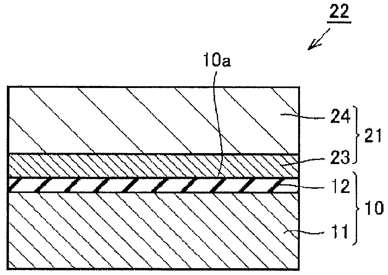
[0076]FIG. 4 is a sectional view schematically showing an epitaxial wafer according to the present embodiment. An epitaxial wafer 20 according to the present embodiment will be described with reference to FIG. 4.
[0077]As shown in FIG. 4, the epitaxial wafer 20 according to the present embodiment includes the III-V compound semiconductor substrate 10 according to the first embodiment and an epitaxial layer 21 disposed on the III-V compound semiconductor substrate 10. That is, the epitaxial wafer 20 includes the substrate 11, the oxide film 21 disposed on the substrate 11, and the epitaxial layer 21 disposed on the oxide film 12.
[0078]The carrier concentration at an interface 10a between the III-V compound semiconductor substrate 10 and the epitaxial layer 21 is preferably less than 5×1014 cm−3, and more preferably 5×1013 cm−3 or less. Since the epitaxial wafer 20 includes the oxide film 12, carriers resulting from the activation of Si can be reduced. Consequently, the above-described...
example 1
[0090]In the present example, an effect resulting from the cleaning step (S12) to clean the substrate with the acidic solution and the formation step (S13) to form the oxide film on the substrate by the wet method was examined.
INVENTION EXAMPLES 1 to 8
[0091]Regarding each of Invention examples 1 to 8, basically, a III-V compound semiconductor substrate was produced following the first embodiment and, thereafter, an epitaxial wafer was produced following the second embodiment.
[0092]Specifically, initially in the preparation step (S11), a GaAs single crystal ingot formed from GaAs was prepared, and a substrate was prepared by slicing the GaAs single crystal ingot. Thereafter, the perimeter of the resulting substrate was chamfered.
[0093]Next, the substrate was subjected to lapping with segregation abrasive grains or grinding with fixed abrasive grains, so that the flatness of the substrate surface was improved and, in addition, the thickness was adjusted. Subsequently, the substrate wa...
PUM
 Abstract
Description
Claims
Application Information
 - R&D Engineer
- R&D Manager
- IP Professional
- Industry Leading Data Capabilities
- Powerful AI technology
- Patent DNA Extraction
Browse by: Latest US Patents, China's latest patents, Technical Efficacy Thesaurus, Application Domain, Technology Topic, Popular Technical Reports.
© 2024 PatSnap. All rights reserved.Legal|Privacy policy|Modern Slavery Act Transparency Statement|Sitemap|About US| Contact US: help@patsnap.com