Controlled power converter
- Summary
- Abstract
- Description
- Claims
- Application Information
AI Technical Summary
Benefits of technology
Problems solved by technology
Method used
Image
Examples
first embodiment
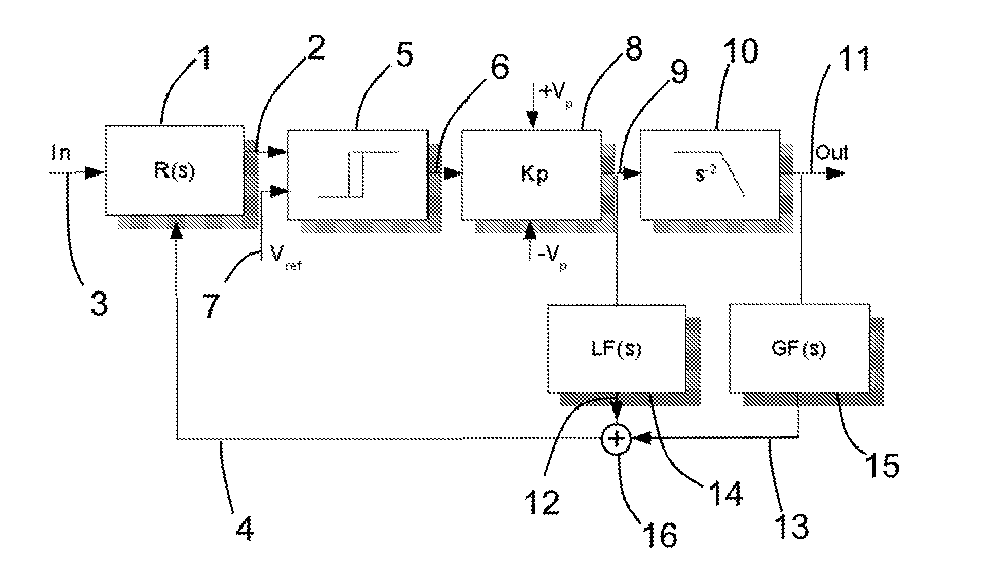
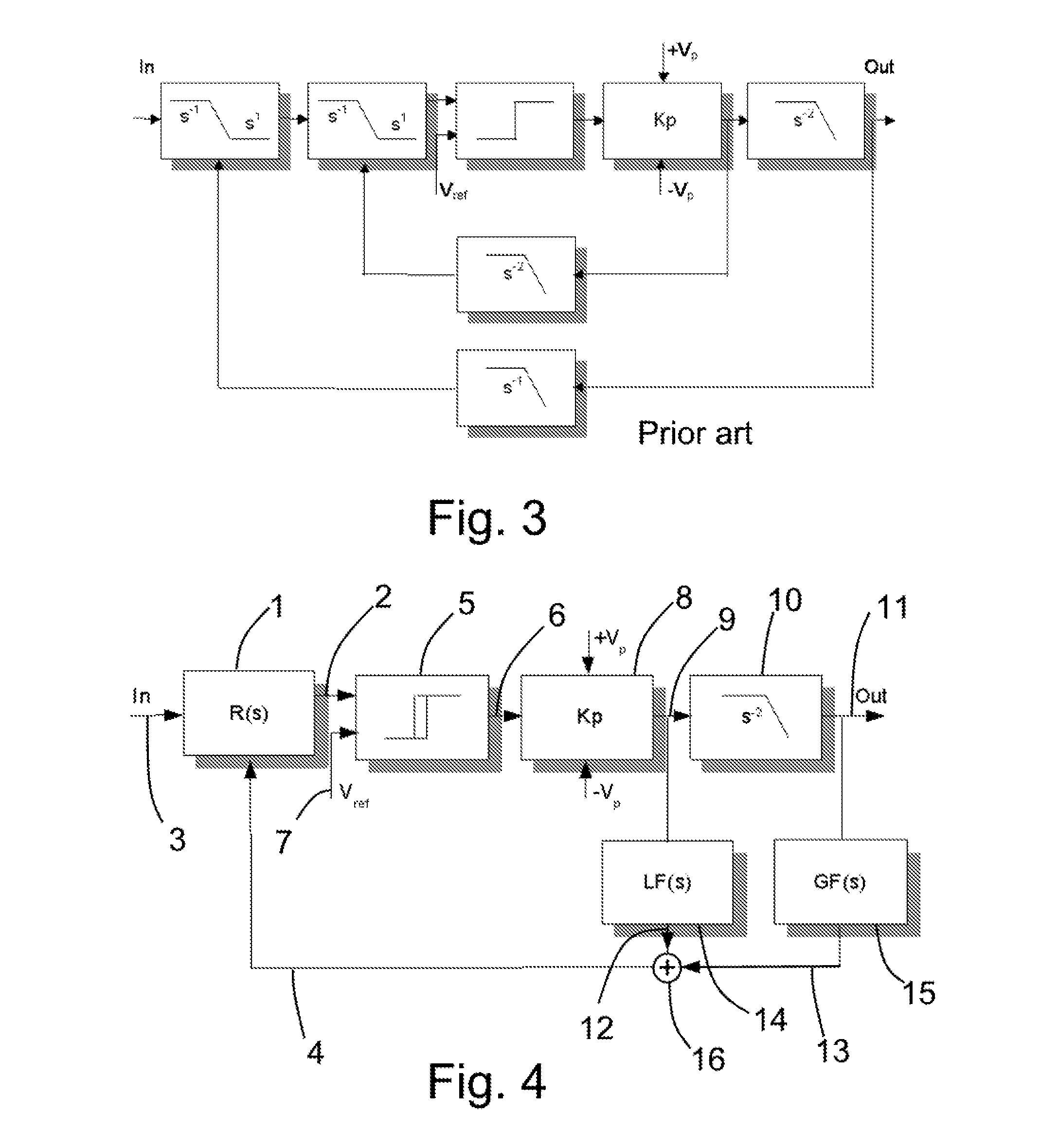
[0046]the invention can be seen from FIG. 4 as a general block diagram of the pulse modulated converter implemented as an amplifier, comprising control and modulator means.
[0047]The pulse modulated converter in FIG. 4 comprises an input signal 3 (In), which is fed into a regulator 1. The regulator 1 can preferably be an integrator or at least comprise a pole. The output signal of the regulator 1 is hereafter termed as the modulating signal or first control signal 2.
[0048]The first control signal 2 is fed to a comparator 5 comparing it to a reference signal 7, such as a reference level (Vref). The comparator 5 for comparing the first control signal 2 to a reference level (Vref) may preferably also incorporate a hysteresis loop for reducing the switching speed and for being able to obtain linear modulation. The comparator 5 forms a pulse signal, such as but not limited to a pulse width modulated signal 6 on the output of said comparator 5.
[0049]The pulse modulated converter further co...
third embodiment
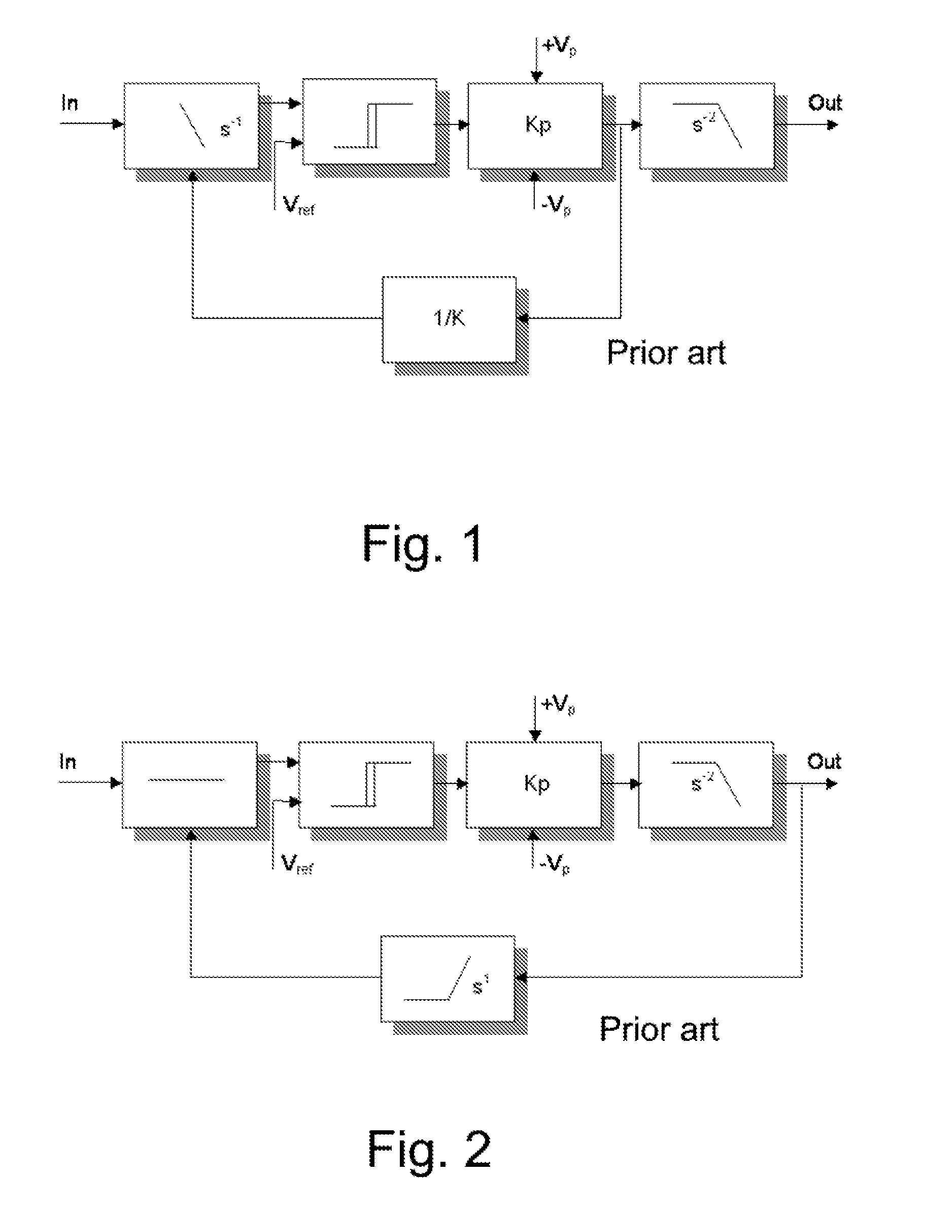
[0069]the invention can be seen from FIG. 6. The first predetermined transfer function 14 of the local loop has been implemented only comprising a gain 1 / K. In order to avoid prohibitive output impedance, the impedance of the local loop must be higher than the DC impedance of the second predetermined transfer function 15 of the global loop. This is important in order to ensure that the error sensitivity at the output of the output filter 10 is low. The DC impedance of the second predetermined transfer function 15 of the global loop should be a factor C smaller than the DC impedance of the first transfer function 34 of the local loop. C should preferably be in the range of 5-10. The regulator 1 can be implemented with at least a pole. The pole can preferably be placed at very low frequencies, so as to obtain an integrating transfer function R(s). If further modulator linearity is needed, the regulator 1 can also comprise at least a zero at higher frequencies, as compared to the pole ...
fourth embodiment
[0071]a pulse modulated converter according to the invention can be seen from FIG. 7. Here, the second predetermined transfer function 15 of the global loop is implemented with a zero in order to have sufficient stability.
[0072]The second predetermined transfer function 15 of the local loop is implemented with a zero and at least 1 pole. This creates a band-pass function in the case where two poles are placed in the second predetermined transfer function 14 of the local loop, or a lead-lag function in the case where only one pole has been implemented. The basis for the local loop feedback signal can be the voltage from the power stage 8 or it can be the current into the output filter inductor. The current can be measured by a traditional current measurement as obvious to the skilled engineer or the voltage can be measured over the output filter inductor and said voltage can then be integrated to provide a virtual current measurement. The current into the output filter inductor will ...
PUM
 Abstract
Description
Claims
Application Information


