Optical scanning device

a scanning device and optical technology, applied in the field of optical scanning devices, can solve the problems of increased manufacturing time, increased manufacturing time, and possible failures, and achieve the effect of reducing variations in optical paths and large siz

Active Publication Date: 2010-01-21
NAT INST OF ADVANCED IND SCI & TECH
View PDF2 Cites 13 Cited by
  • Summary
  • Abstract
  • Description
  • Claims
  • Application Information

AI Technical Summary

Benefits of technology

[0063]The invention provides the excellent effects described below.(1) By supporting both sides of a mirror portion using torsion bar portions between two cantilever beam portions which protrude from two end sides of a substrate main body, and fixing the end portion of the substrate main body located on the opposite side from the mirror portion side, and by also providing a drive source in a portion of the substrate main body, it is possible to provide a high-performance optical scanning device which has a fast scanning speed that is greater than or equal to 5 kHz and has a large amplitude optical scan angle that is greater than or equal to 20°. Moreover, torsional vibration is possible in the mirror portion irrespective of whether the mirror portion is supported at the center of gravity thereof or at a position away from the center of gravity thereof. Furthermore, it is possible to achieve a simplification of the structure and a reduction in manufacturing costs. In addition, it is possible to impart a large vibration to the mirror portion using only a small-sized vibration source. Furthermore, it is possible to considerably reduce the power consumption of the piezoelectric element forming the vibration source. Moreover, because there is an increased degree of freedom in the placement of the piezoelectric element, it is possible to achieve a reduction in both the size and the thickness of the optical scanning device.(2) By fixing the fixed end portion of the substrate main body located on the opposite side thereof from the mirror portion side within a range of 1 / 20 to ¾ the width of the substrate main body, and by forming the cross-sectional configuration of the fixed end portion in a curved shape or in a bent shape, and by making the thickness of the film body less than or equal to 6 times the thickness of the substrate, and by making the surface area of the film body less than or equal to ¾ the surface area of the substrate main body, it is possible to obtain an optical scanning device which has a superior fast scanning speed and large amplitude optical scan angle.(3) By placing the connecting portions where the torsion bar portions which support the mirror portion connect to the cantilever beam portions in the vicinity of the minimum amplitude (i.e., the bottom point of the amplitude) of the substrate vibration excited in the substrate main body by the film body, it is possible to impart a large rotational moment to the mirror portion and efficiently excite torsional vibration.
[0064]At this time, in order to excite torsional vibration in the mirror portion, it is necessary for the adjacent distance between the above-described bottom point of the vibration, which is the minimum amplitude of the substrate vibration, and the connecting portions to be less than or equal to ±¼ the plate wave wavelength (λ). In addition, in order to suppress variations in the optical path of the optical system which are due to the shafts of the torsion bar portions supporting the mirror portion vibrating vertically to a minimum and to a practical level, and obtain a large torsional vibration in the mirror portion, it is desirable for the above-described adjacent distance to be less than or equal to ±⅙, and even more desirably to be less than or equal to ±⅛.(4) Furthermore, by providing the connecting portions between the substrate portion and the cantilever beam portions 19 which support the torsion bar portions 12 which are connected to the mirror portion 13 in the vicinity of the maximum amplitude of the substrate vibration (i.e., in the middle of the vibration) which is excited by the drive source in the substrate main body, it is possible to efficiently impart excitation energy to the cantilever beam portions, and impart a large rotational moment to the mirror portion, and efficiently excite torsional vibration.(5) By setting by a considerable amount the resonance frequency of the mirror portion which is determined by the mass of the mirror portion and by the spring constant of the torsion bars away from the resonance frequency of the substrate, it is possible to transmit vibration energy generated at a position separated from the mirror portion efficiently as energy which generates torsional vibration in the mirror portion.(6) By positioning a substrate fixing frame so as to surround the substrate main body and cantilever beam portions and then fixing it on the fixed end portion side of the substrate main body, and by connecting together the substrate main body and the substrate fixing frame by means of substrate connecting bars at a position away from the supporting component and also in the vicinity of the minimum amplitude of the substrate vibration, it is possible to stably support the optical scanning device against external disturbance vibration without attenuating the scan amplitude of the mirror portion.

Problems solved by technology

In this manner, because the electrode portion 5 is formed on at least peripheral areas or on the surface of the mirror 2, and the pads 4a and 4b are formed on the torsion bars 3a and 3b, and the respective fixed electrodes 7a and 7b and pads 8a and 8b are formed at positions on both sides of the surface of the supporting substrate 1 via the insulator 6, the manufacturing of this optical scanning device is complex, and not only have the causes for possible failures increased, but the time required for manufacturing has also increased.
Accordingly, there is a problem in that cost increases.
Moreover, the device also needs to have a certain thickness not only in the X-Y axial directions, but also in the Z axial direction, so that it is difficult for this device to be manufactured with a slender thickness.
Moreover, the optical scanning device of the above-described Conventional technology 3 has the drawback that a large torsion angle cannot be formed in the movable portion 2.
Namely, if a piezoelectric film is formed in the two narrow cantilever beam portions which support the two torsion bars protruding from the frame portion, then the rigidity of this portion increases and vibration which is induced in the piezoelectric film is not transmitted efficiently to the torsion bars.
Moreover, unless the vibration characteristics of the vibration source portion formed by the two cantilever beam portions and the piezoelectric film which is formed thereon are matched precisely, then the vibration amplitude of the torsional vibration of the mirror becomes suppressed and, at the same time as this, torsion modes other than torsional vibration are superimposed thereon so that accurate laser beam scanning cannot be achieved.
As a result, there is a problem in that it is not possible to achieve accurate laser beam scanning.
Moreover, because the width of the cantilever beams is restricted to a narrow width, the formation of the top portion electrodes which are used to drive the piezoelectric film formed on this portion is made more difficult because of the narrow width, so that problems arise such as the yield during production being greatly affected.

Method used


Image

  • Optical scanning device
  • Optical scanning device
  • Optical scanning device

Examples


example 1

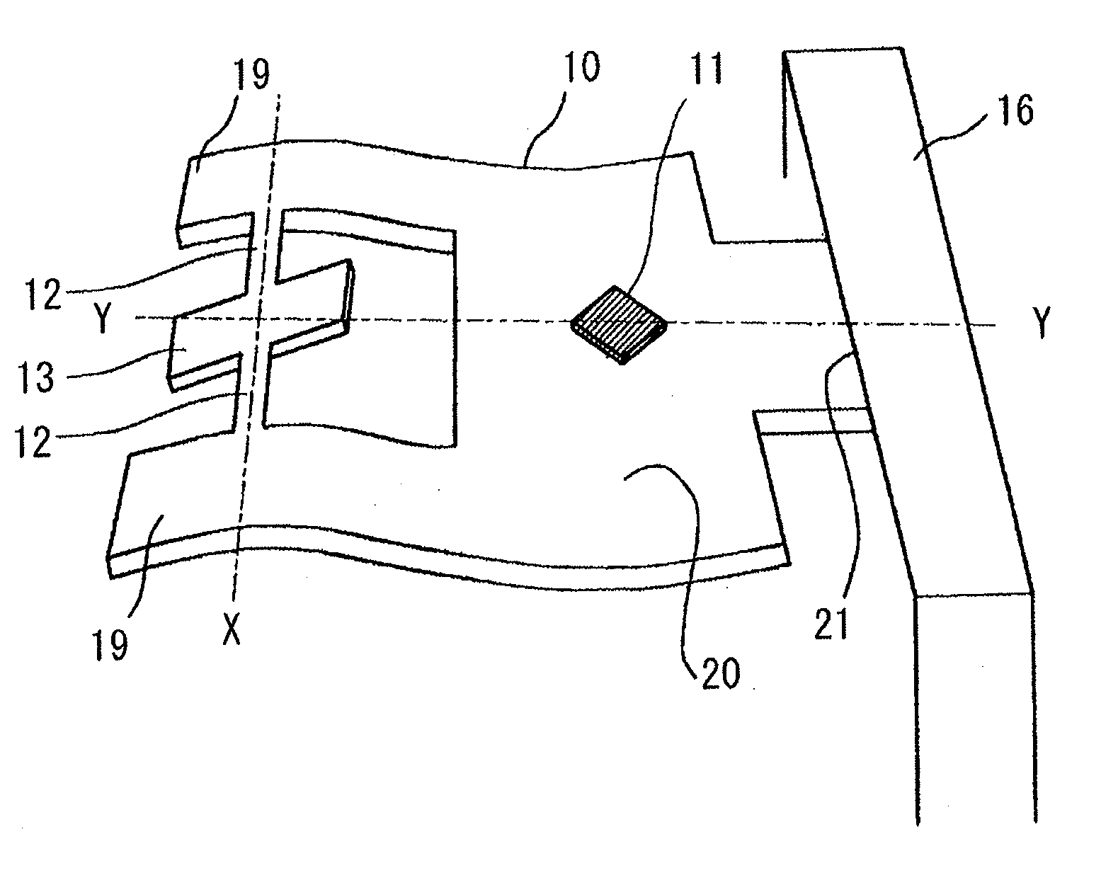
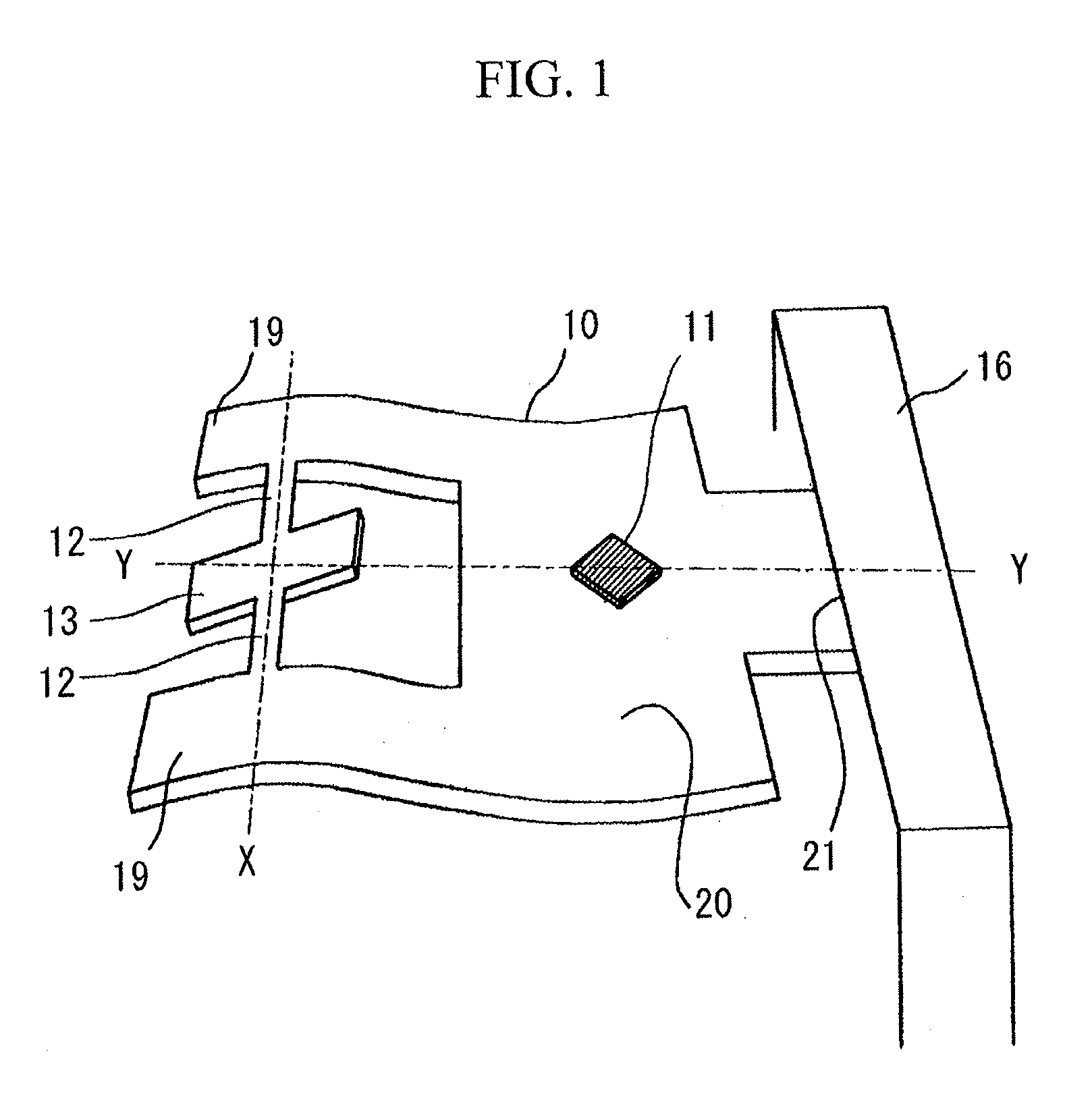
[0092]FIG. 12 is a perspective view showing an optical scanning device according to Example 1.

[0093]A substrate 10 is manufactured by etching or by press working a square plate material of SUS 304 having a thickness of 30 or 50 μm such that the substrate 10 is cut out so as to leave torsion bar portions 12 and a mirror portion 13 remaining. The substrate 10 is formed by a substrate main body 20 and cantilever beam portions 19 and 19 which protrude in parallel with each other from two sides of one side of the substrate main body 20. The torsion bar portions 12 which support the mirror portion 13 are provided extending in an orthogonal direction relative to the axial direction of the two cantilever beam portions 19 and 19.

[0094]A fixed end portion 21 which is located on the opposite side from the mirror portion 13 side of the substrate main body 20 is fixed by means of a supporting component 16, so as to form a structure in which the substrate 10 is supported in cantilever fashion by ...


PUM


Abstract

An optical scanning device of the invention includes: a substrate main body;two cantilever beam portions which protrude from both-side portions of one side of the substrate main body; a mirror portion whose both-sides are supported by torsion bar portions between the cantilever beam portions; a drive source which causes the substrate main body to oscillate; and a light source which projects light onto the mirror portion, where the mirror portion resonates and vibrates in accordance with a vibration imparted to a substrate by the drive source, and a direction of reflection light from the light projected onto the mirror portion from the light source changes in accordance with the vibration of the mirror portion, and where a fixed end portion of the substrate main body which is located on the opposite side thereof from the mirror portion side is fixed to a supporting component, and the drive source is provided on a portion of the substrate main body.

Description

BACKGROUND OF THE INVENTION[0001]1. Field of the Invention[0002]The present invention relates to an optical scanner which performs scans by the scanning of an optical beam, and, in particular, to an optical scanning device having a structure in which a micro mirror which is supported by torsion bars is made to oscillate so as to cause the direction of an optical beam to change.[0003]2. Background Art[0004]In recent years, optical scanners which scan optical beams of laser light or the like have been used as optical instruments such as bar code readers, laser printers, and head mounted displays, or as the optical intake devices of input devices such as infrared cameras and the like. Optical scanners having a structure in which a micro mirror obtained via silicon micromachining technology is oscillated have been proposed for this type of optical scanner. For example, FIG. 22 shows an optical scanner having a silicon micro mirror which is disclosed in Japanese Unexamined Patent Applica...

Claims


Application Information

Patent Timeline
Patent Type & Authority Applications(United States)
IPC IPC(8): G02B26/10
CPCG02B26/105G02B26/0833B81B3/00G02B26/08G02B26/10
Inventor AKEDO, JUNSATO, HARUMICHIPARK, JAEHYUK
Owner NAT INST OF ADVANCED IND SCI & TECH
Why Eureka
Try Eureka