Epitaxial substrate for field effect transistor

a field effect transistor and substrate technology, applied in the direction of basic electric elements, electrical appliances, semiconductor devices, etc., can solve the problems of deterioration of pinch-off characteristics, increased drain leakage, and low and achieve the effect of reducing the mobility of unnecessary current components and reducing the number of transistors

Inactive Publication Date: 2010-01-28
SUMITOMO CHEM CO LTD
View PDF14 Cites 17 Cited by
  • Summary
  • Abstract
  • Description
  • Claims
  • Application Information

AI Technical Summary

Benefits of technology

[0018]An object of the present invention is to provide an epitaxial substra

Problems solved by technology

This leads to the problems of deterioration of pinch-off characteristics and increase in drain leakage.
Furthermore, the unnecessary current component has low mobility different from 2DEG.
As a result, in the case of operating the gate electrode with high frequency voltage, adverse influence such as frequency dispersion is involved.
Additionally, the unfavorable unnecessary current also flows into adjacent other elements, causing the interference such as fluctuation of threshold voltage of the adjacent elements.
In general, nitride-based Group III-V monocrystal has extremely high stability chemically and physically, and deep element isolation processing as reaching the substrate is extremely difficult.
However, it is not easy to epitaxially grow high resistivity nitride Group III-V monocrystal.
Various crystal defects are present in crystal.
However, the above-described prior arts have the following problems on production.
It is known that beryllium has extremely stron

Method used


Image

  • Epitaxial substrate for field effect transistor
  • Epitaxial substrate for field effect transistor
  • Epitaxial substrate for field effect transistor

Examples


example 1

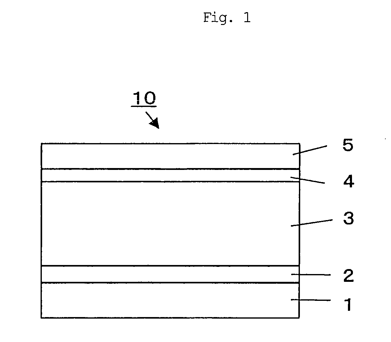
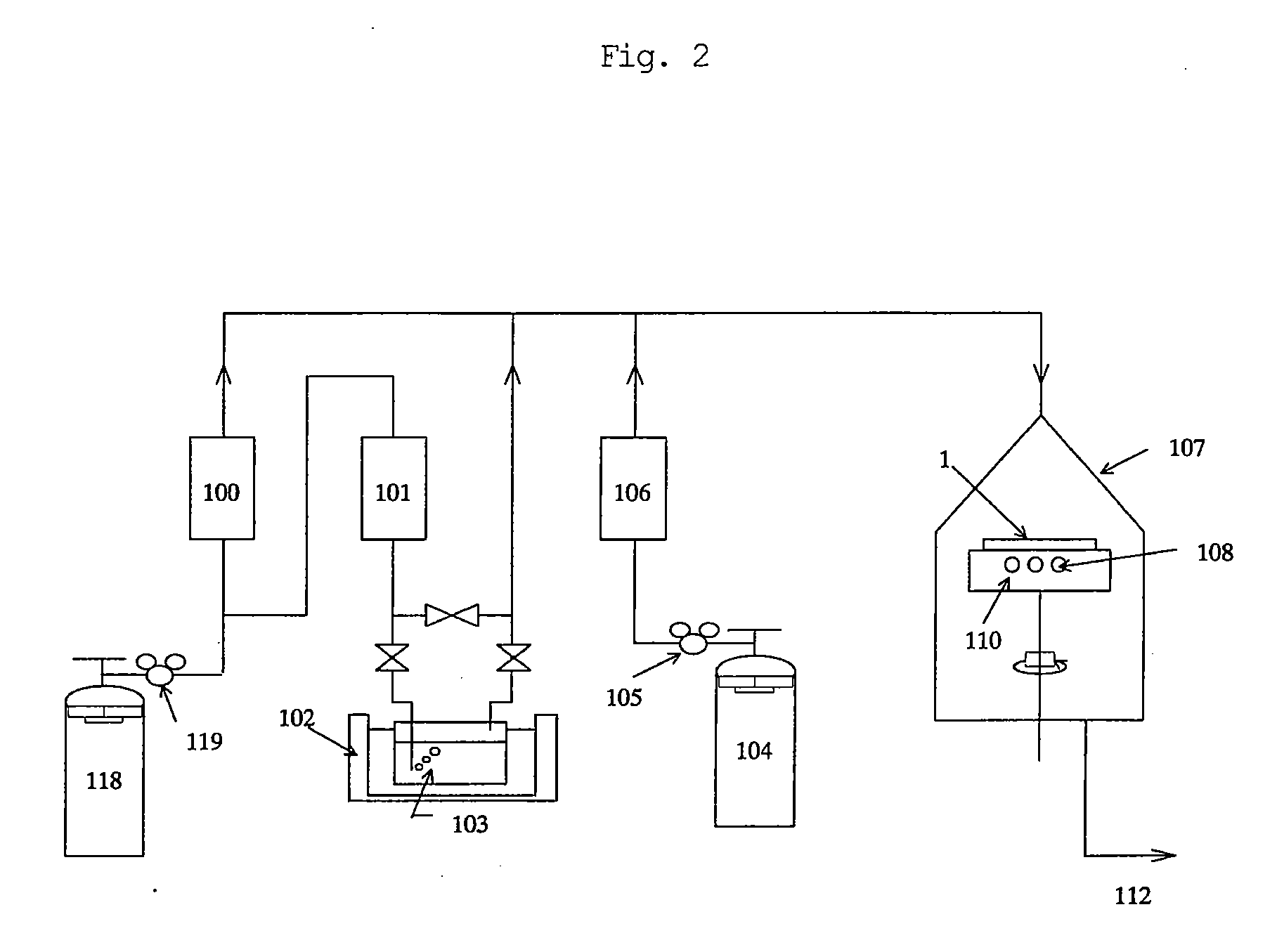
[0088]Using the apparatus shown in FIG. 2, an epitaxial substrate for FET having the layer structure shown in FIG. 1 was prepared as follows. A sapphire monocrystal substrate was heated to 600° C., hydrogen as a carrier gas was allowed to flow in an amount of 60 SLM, ammonia was allowed to flow in an amount of 40 SLM, TMA was allowed to flow in an amount of 40 sccm from a container in a temperature-controlled bath set to a temperature of 30° C., and biscyclopentadienyl was allowed to flow from a container in a temperature-controlled bath set to a temperature of 30° C. (0 sccm in sample (a), 200 sccm in sample (b) and 1,000 sccm in sample (c)). Thus, AlN first buffer layer was grown to a thickness of 500 angstroms. Growth rate in this case was 470 angstroms / min.

[0089]The substrate temperature was increased to 1,040° C., and the flow rate of TMA was changed to 0 sccm. Then, TMG was allowed to flow in an amount of 40 sccm from a container in a temperature-controlled bath set to a tempe...

example 2

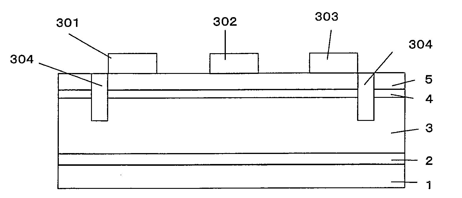
[0091]Using the apparatus shown FIG. 2, GaN-HEMT having the layer structure shown in FIG. 3 was prepared. In FIG. 3, the parts corresponding to the respective parts in FIG. 1 are indicated by the same reference numerals. A sapphire monocrystal substrate as the ground substrate 1 was heated to 600° C., hydrogen as a carrier gas was allowed to flow in an amount of 60 SLM, ammonia was allowed to flow in an amount of 40 SLM, TMA was allowed to flow in an amount of 40 sccm from a container in a temperature-controlled bath set to a temperature of 30° C., and biscyclopentadienyl was allowed to flow from a container in a temperature-controlled bath set to a temperature of 30° C. (0 sccm in sample (d), and 1,000 sccm in samples (e) and (f)) Thus, AlN first buffer layer 2 was grown to a thickness of 500 angstroms. Growth rate in this case was 470 angstroms / min.

[0092]The substrate temperature was increased to 1,040° C., and the flow rate of TMA was changed to 0 sccm. TMG was allowed to flow in...


PUM


Abstract

The present invention provides an epitaxial substrate for field effect transistor. In the epitaxial substrate for field effect transistor, a nitride-based Group III-V semiconductor epitaxial crystal containing Ga is interposed between the ground layer and the operating layer, and the nitride-based Group III-V semiconductor epitaxial crystal comprises the following (i), (ii) and (iii). (i) a first buffer layer containing Ga or Al and containing a high resistivity crystal layer having added thereto compensation impurity element present in the same period as Ga in the periodic table and having small atomic number; (ii) a second buffer layer containing Ga or Al, laminated on the operating layer side of the first buffer layer; and (iii) a high purity epitaxial crystal layer containing acceptor impurities in a slight amount such that non-addition or depletion state can be maintained, provided between the high resistivity layer and the operating layer.

Description

TECHNICAL FIELD[0001]The present invention relates to an epitaxial substrate for field effect transistor (hereinafter referred to as “FET”) using a nitride-based Group III-V semiconductor.BACKGROUND ART[0002]A field effect transistor using a nitride-based Group III-V semiconductor epitaxial substrate (hereinafter referred to as “GaN-FET”) is a field effect transistor constituted such that a GaN layer drives as a channel layer, and it is an element which rapidly becomes widely noticed of late from that the GaN-FET has high voltage resistance, high heat resistance and small environmental load of constituent materials as compared with the conventional FET having a structure that an epitaxial semiconductor crystal layer such as GaAs, AlGaAs, InGaAs, InGaP and AlInGaP is used as a channel layer.[0003]The GaN-FET has various types in view of the structure of an operating layer. In particular, the GaN-FET of the type that a two-dimensional electron gas (hereinafter referred to as “2DEG”) i...

Claims


Application Information

Patent Timeline
IPC IPC(8): H01L29/20
CPCH01L21/0242H01L21/02458H01L21/02502H01L21/0254H01L29/7783H01L21/0262H01L29/2003H01L29/207H01L29/66462H01L21/02581H01L21/18H01L21/205H01L29/778
Inventor HATA, MASAHIKOSAZAWA, HIROYUKINISHIKAWA, NAOHIRO
Owner SUMITOMO CHEM CO LTD
Why Eureka
Try Eureka