Method for manufacturing soi substrate

a technology of silicononinsulator and substrate, which is applied in the direction of semiconductor/solid-state device manufacturing, basic electric elements, electric apparatus, etc., can solve the problems of damage to the planarity of the separated bond substrate, inability to sufficiently bond glass substrate and a bond substrate to each other, and inability to achieve uniform thickness. uniformity,

Inactive Publication Date: 2010-01-28
SEMICON ENERGY LAB CO LTD
View PDF13 Cites 29 Cited by
  • Summary
  • Abstract
  • Description
  • Claims
  • Application Information

AI Technical Summary

Problems solved by technology

However, many crystal defects are formed on a surface of the separated bond substrate from which a thin semiconductor film has been separated by Smart Cut and the planarity of the separated bond substrate is damaged severely.
In particular, there is a problem in that in the case of using substrates of which coefficients of thermal expansion are different from each other, such as using a glass substrate as a base substrate and using as a single crystal silicon substrate as a bond substrate, on separation surfaces of a semiconductor film bonded to the glass substrate and the separated bond substrate, a thickness non-uniformity is formed.
There may be a problem in that, for example, in the case of reusing a bond substrate having a thickness non-uniformity on the surface for manufacturing an SOI substrate, a glass substrate and a bond substrate cannot be sufficiently bonded to each other.
However, since a CMP method is a method in which a substrate surface is polished mechanically, there is a problem in that a polished portion (an amount of polishing) of the bond substrate is increased.
That is, a removed portion of the bond substrate is increased in a reprocessing treatment process, and thus the number of reprocessing and using one bond substrate is reduced, which leads to an increase in cost.
In particular, in a peripheral portion of a bond substrate such as a commercial single crystal silicon wafer, there is a chamfer portion where a corner is chamfered in a peripheral portion; therefore, the peripheral portion of the bond substrate cannot be bonded to a glass substrate favorably.

Method used


Image

  • Method for manufacturing soi substrate
  • Method for manufacturing soi substrate
  • Method for manufacturing soi substrate

Examples


embodiment 1

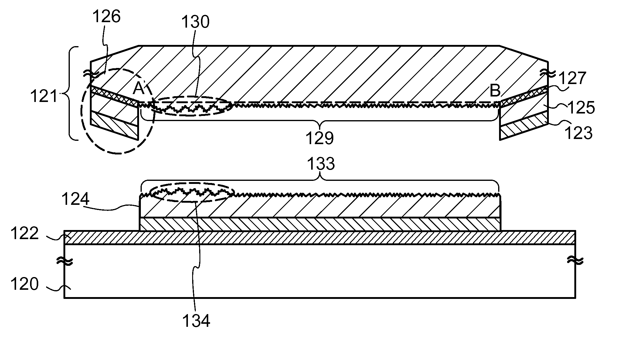
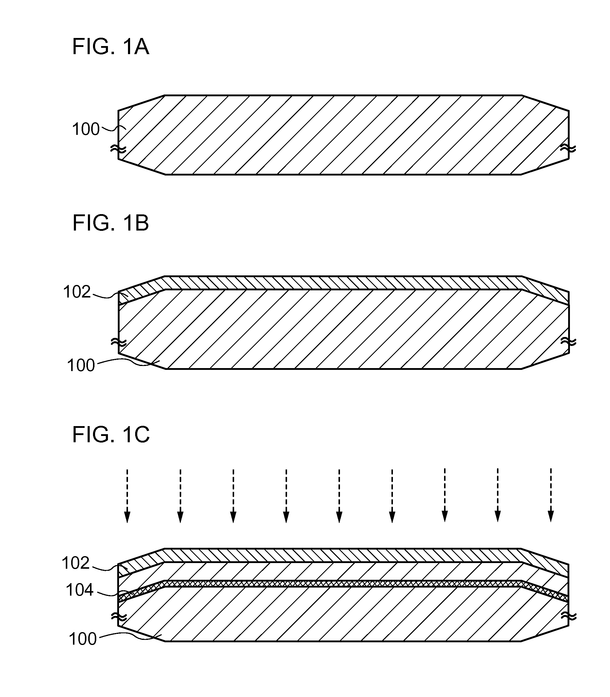
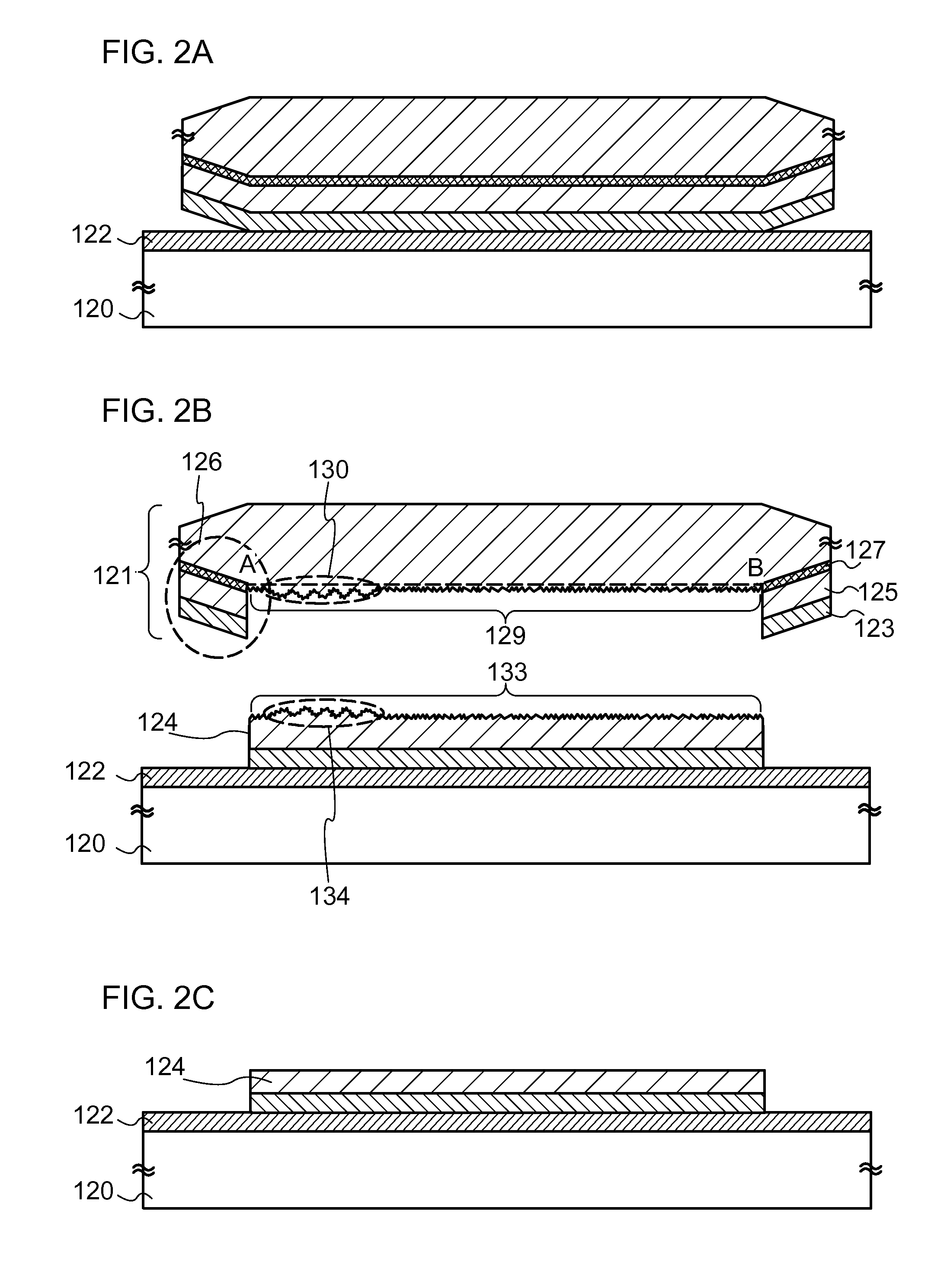
[0040]In a method for manufacturing an SOI substrate according to this embodiment, an SOI substrate is manufactured in such a manner that a semiconductor film separated from a semiconductor substrate which is a bond substrate is bonded to a base substrate. The separated bond substrate from which the semiconductor film has been separated is subjected to reprocessing treatment and reused as a bond substrate. Hereinafter, with reference to FIGS. 1A to 1C, FIGS. 2A to 2C, FIGS. 3A to 3C, FIGS. 4A to 4C, FIG. 5, and FIG. 6 which illustrate steps of manufacturing an SOI substrate, one of methods for manufacturing an SOI substrate of this embodiment will be described.

[0041]First, a process of forming an embrittlement layer 104 in a bond substrate 100 and preparing for bonding the bond substrate 100 to a glass substrate 120 which is a base substrate will be described. The following process corresponds to Process A (bond substrate process) in FIG. 6.

[0042]First, the bond substrate 100 as ill...

embodiment 2

[0120]In this embodiment, a method for manufacturing a semiconductor device by using the SOI substrate manufactured according to the above embodiment will be described. Note that a process described in this embodiment corresponds to a process F (a device process) in FIG. 6.

[0121]First, with reference to FIGS. 7A to 7D and FIGS. 8A to 8C, a method for manufacturing an n-channel thin film transistor and a p-channel thin film transistor will be described. Various kinds of semiconductor devices can be formed by combining a plurality of thin film transistors (TFTs).

[0122]The case where the SOI substrate manufactured by the method of Embodiment 1 is used as an SOI substrate will be described. FIG. 7A is a cross-sectional view of the SOI substrate in FIG. 2C.

[0123]The semiconductor film 124 is separated into each element by etching to form a semiconductor film 251 and a semiconductor film 252 as illustrated in FIG. 7B. The semiconductor film 251 is included in an n-channel TFT, and the sem...

embodiment 3

[0135]In this embodiment, specific modes of a semiconductor device manufactured by using an SOI substrate described in the above embodiment will be described with reference to FIG. 9 and FIG. 10.

[0136]First, a microprocessor will be described as an example of a semiconductor device. FIG. 9 is a block diagram illustrating a structural example of a microprocessor 500.

[0137]The microprocessor 500 has an arithmetic logic unit (also referred to as an ALU) 501, an ALU controller 502, an instruction decoder 503, an interrupt controller 504, a timing controller 505, a register 506, a register controller 507, a bus interface (Bus I / F) 508, a read only memory (ROM) 509, and a ROM interface 510.

[0138]An instruction input to the microprocessor 500 via the bus interface 508 is input to the instruction decoder 503 and decoded. Then, the instruction is input to the ALU controller 502, the interrupt controller 504, the register controller 507, and the timing controller 505. The ALU controller 502, ...


PUM

PropertyMeasurementUnit
thicknessaaaaaaaaaa
diameteraaaaaaaaaa
diameteraaaaaaaaaa

Abstract

It is an object to provide a method for, after a semiconductor film is separated, reprocessing a separated bond substrate into a reprocessed bond substrate which can be used for manufacturing an SOI substrate. The method for, after a semiconductor film is separated, reprocessing a separated bond substrate into a reprocessed bond substrate which can be used for manufacturing an SOI substrate includes the steps of forming an insulating film over a bond substrate; adding ions from a surface of the bond substrate to form an embrittlement layer; bonding the bond substrate to a glass substrate with the insulating film interposed therebetween; separating, at the embrittlement layer, the bond substrate into a semiconductor film which is bonded to the glass substrate with the insulating film interposed therebetween and a separated bond substrate; performing first wet etching using a solution containing hydrofluoric acid as an etchant on the separated bond substrate; performing second wet etching using an organic alkaline aqueous solution as an etchant on the separated bond substrate; performing thermal oxidation treatment on the separated bond substrate in an oxidizing atmosphere to which a gas containing halogen is added to form an oxide film on a surface of the separated bond substrate; performing third wet etching using a solution containing hydrofluoric acid as an etchant on the oxide film; and forming a reprocessed bond substrate by performing polishing on the separated bond substrate.

Description

BACKGROUND OF THE INVENTION[0001]1. Field of the Invention[0002]The present invention relates to a method for manufacturing a silicon-on-insulator (SOI) substrate.[0003]2. Description of the Related Art[0004]In recent years, integrated circuits using a silicon-on-insulator (SOI) substrate in which a thin single crystal semiconductor layer is provided on an insulating surface, instead of a bulk silicon wafer, have been developed. By utilizing characteristics of the thin single crystal silicon film formed on the insulating surface, transistors in the integrated circuit can be separated from each other completely. Further, since the transistors can be formed as fully depleted transistors, a semiconductor integrated circuit with high added value such as high integration, high-speed driving, and low power consumption can be realized.[0005]As one of methods for manufacturing an SOI substrate, Smart Cut (registered trademark) can be given. By using Smart Cut, an SOI substrate having a sing...

Claims


Application Information

Patent Timeline
Patent Type & Authority Applications(United States)
IPC IPC(8): H01L21/762
CPCH01L21/76254
Inventor IMAHAYASHI, RYOTA
Owner SEMICON ENERGY LAB CO LTD
Why Eureka
Try Eureka