High q transformer disposed at least partly in a non-semiconductor substrate

Active Publication Date: 2010-02-04
QUALCOMM INC
View PDF13 Cites 52 Cited by
  • Summary
  • Abstract
  • Description
  • Claims
  • Application Information

AI Technical Summary

Benefits of technology

[0007]In one specific example, the non-semiconductor substrate is a multi-layer interconnect structure that includes several layers of metal interconnect and several layers of a non-semiconductor dielectric material. The integrated circuit die is an RF transceiver integrated circuit die that includes a mixer and a driver amplifier in a transmit chain of a radio transmitter circuit. The mixer drives the driver amplifier through the transformer. Part of the novel transformer is disposed in the integrated circuit die, thereby allowing small conductor widths and geometries to be used such that a high degree of coupling is achieved between the p

Problems solved by technology

Prior art integrated transformer structures, for example such as the structures illustrated in FIGS. 2 and 3, generally have either an undesirabl

Method used


Image

  • High q transformer disposed at least partly in a non-semiconductor substrate
  • High q transformer disposed at least partly in a non-semiconductor substrate
  • High q transformer disposed at least partly in a non-semiconductor substrate

Examples


Embodiment Construction

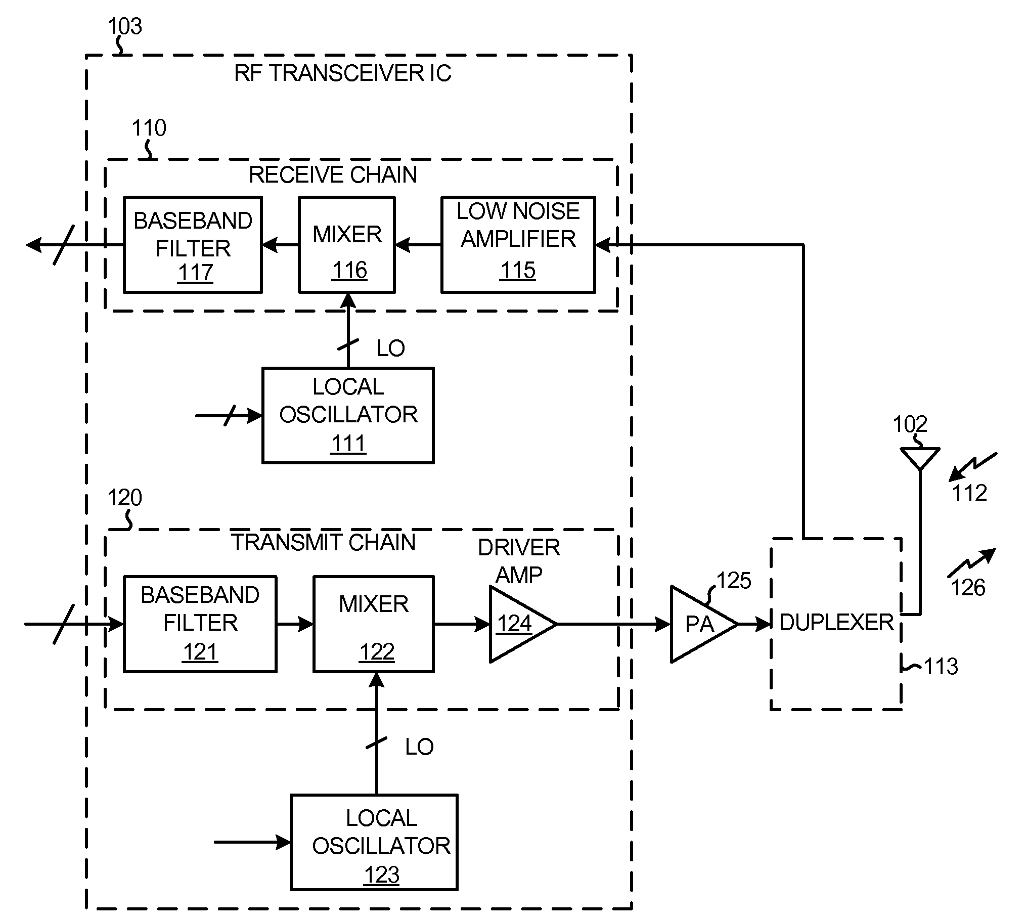
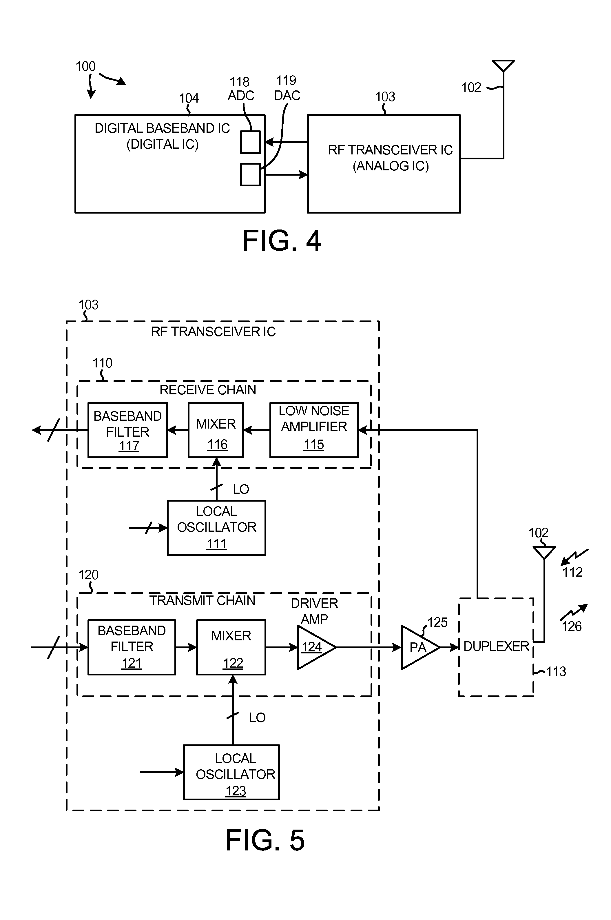
[0032]FIG. 4 is a very simplified high level block diagram of one particular type of mobile communication device 100 in accordance with one novel aspect. In this particular example, mobile communication device 100 is a 3G cellular telephone capable of operating in accordance with a Code Division Multiple Access (CDMA) cellular telephone communication protocol. The cellular telephone includes (among several other parts not illustrated) an antenna 102 and two integrated circuits 103 and 104. Integrated circuit 104 is called a “digital baseband integrated circuit” or a “baseband processor integrated circuit”. Integrated circuit 103 is an RF transceiver integrated circuit. RF transceiver integrated circuit 103 is called a “transceiver” because it includes a transmitter as well as a receiver.

[0033]FIG. 5 is a more detailed block diagram of the RF transceiver integrated circuit 103 of FIG. 5. The receiver includes what is called a “receive chain”110 as well as a local oscillator 111. When...


PUM


Abstract

An assembly involves an integrated circuit die that is bonded, e.g., flip-chip bonded, to a non-semiconductor substrate by a plurality of low-resistance microbumps. In one novel aspect, at least a part of a novel high-frequency transformer is disposed in the non-semiconductor substrate where the non-semiconductor substrate is the substrate of a ball grid array (BGA) integrated circuit package. At least one of the low-resistance microbumps connects the part of the transformer in the substrate to a circuit in the integrated circuit die. At two gigahertz, the novel transformer has a coupling coefficient k of at least at least 0.4 and also has a transformer quality factor Q of at least ten. The novel transformer structure sees use in coupling differential outputs of a mixer to a single-ended input of a driver amplifier in a transmit chain of an RF transceiver within a cellular telephone.

Description

BACKGROUND INFORMATION[0001]1. Technical Field[0002]The disclosed embodiments relate to transformers for high frequency applications.[0003]2. Background Information[0004]Radio frequency (RF) circuits such as transceivers found in cellular telephones often involve inductors and transformers. FIG. 1 (Prior Art) is a top-down view of a spiral-shaped inductor 21 disclosed in U.S. Pat. No. 6,180,445. Spiral-shaped inductor 21 is fabricated on a silicon substrate along with active devices in an active region of the silicon substrate. An inductor may also be partly disposed in a non-semiconductor substrate and connected by a microbump to circuitry in an IC, which can then be flip-chip bonded to a BGA package substrate.[0005]U.S. Pat. No. 6,833,285 shows another example of a spiral-shaped inductor that is fabricated on a silicon substrate. The structure is part of a flip-chip silicon interposer. FIG. 2 (Prior Art) is a top-down view of a flip-chip transformer 16 that is disclosed in U.S. Pu...

Claims


Application Information

Patent Timeline
IPC IPC(8): H01F27/28G06G7/14
CPCH01L23/48H01L23/49534H01L23/50H01L23/5227H01L2924/01019H01L2924/01079H01L2924/15311H01L2924/3011H01L2224/16H01L2924/00014H01L2924/00011H01L2224/0401H01L23/52
Inventor TANG, YIWUJIN, ZHANG
Owner QUALCOMM INC
Why Eureka
Try Eureka