Display Drive Systems

a technology of display drive and drive voltage, which is applied in the direction of cathode-ray tube indicators, instruments, electric digital data processing, etc., can solve the problems of pixels burning in, drive voltage, and difficulty in predicting how bright a pixel will appear when driven by a given voltag

Inactive Publication Date: 2010-02-04
CAMBRIDGE DISPLAY TECH LTD
View PDF26 Cites 146 Cited by
  • Summary
  • Abstract
  • Description
  • Claims
  • Application Information

AI Technical Summary

Benefits of technology

[0037]In embodiments the extra transistor of the pixel driver circuit need not be implemented in every pixel of an active matrix display, but only on a few of the pixels, that is those for which voltage drop measurements are desired. In embodiments the pixel driver circuit is implemented in a row (or column) of the display and the second electrode line comprises a power su...

Problems solved by technology

In a voltage-controlled configuration the brightness can vary across the area of a display and with time, temperature, and age, making it difficult to predict how bright a pixel will appear when driven by a given voltage.
One problem associated with OLED displays is that, over time, the pixels “burn-in”, that is the drive voltage required for a given drive current (and hence luminosity) increases with use.
Thus two different but related problems can arise from burn-in: firstly a general aging of the display with use, and secondly image burn-in, where per...

Method used


Image

  • Display Drive Systems
  • Display Drive Systems
  • Display Drive Systems

Examples


Embodiment Construction

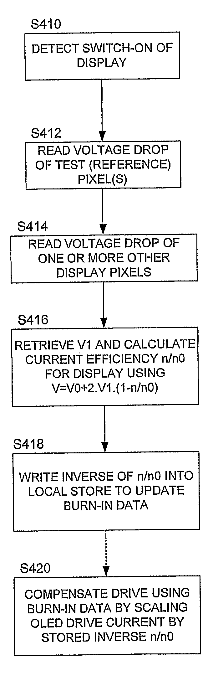
[0047]Referring to FIGS. 4a and 4b these show, respectively, the efficiency of an OLED (in candelas per amp) and the drive voltage of an OLED (in volts) against driven time (in hours). Both graphs have been fitted with the same stretched exponential function,

exp-(tτ)nor1-exp-(tτ)n

and it can be seen that there is a strong correlation between the fall-off in efficiency of the OLED device and the increased drive voltage needed for the same drive current / light output. The drive voltage, V, can be expressed as follows:

V=V0=2V1(1-ηη0)(1)

where V0 and η0 are the voltage and efficiency at time t=0, and V1 is the end-of-life voltage increase. As previously mentioned in embodiments of the invention we arbitrarily define the end-of-life as the half-efficiency point so that in Equation (1) above at the end-of-life point η / η0=½ and thus V=V0+V1.

[0048]In Equation (1) V0 is dependent upon the temperature, T, of the OLED device and may be specified, for example, at 25° C.; to make this clearer V0 ma...


PUM


Abstract

This invention generally relates to methods, apparatus and computer program code for improved OLED (organic light emitting diode) display drive systems, in particular to compensate for burn-in.
A method of compensating an OLED display device for burn-in of pixels of the OLED display, the method comprising: measuring a first voltage drop across at least one test pixel of the display; measuring a second voltage drop across at least one other pixel of the display; determining, from said first and second voltages and a from value (V1) representing a drive voltage increase for a loss in efficiency of said display due to burn-in, an estimated reduction in efficiency of said display due to burn-in; and compensating a drive to said display using said estimated efficiency reduction.

Description

[0001]This invention generally relates to methods, apparatus and computer program code for improved OLED (organic light emitting diode) display drive systems, in particular to compensate for burn-in.[0002]Organic light emitting diodes, which here include organometallic LEDs, may be fabricated using materials including polymers, small molecules and dendrimers, in a range of colours which depend upon the materials employed. Examples of polymer-based organic LEDs are described in WO 90 / 13148, WO 95 / 06400 and WO 99 / 48160; examples of dendrimer-based materials are described in WO 99 / 21935 and WO 02 / 067343; and examples of so called small molecule based devices are described in U.S. Pat. No. 4,539,507. A typical OLED device comprises two layers of organic material, one of which is a layer of light emitting material such as a light emitting polymer (LEP), oligomer or a light emitting low molecular weight material, and the other of which is a layer of a hole transporting material such as a ...

Claims


Application Information

Patent Timeline
IPC IPC(8): G09G5/10G09G5/00
CPCG09G3/3216G09G3/3233G09G3/3241G09G2320/048G09G2320/029G09G2320/043G09G2320/045G09G2300/0842G09G3/3208G09G3/20G09G3/30
Inventor SMITH, EUAN
Owner CAMBRIDGE DISPLAY TECH LTD
Why Eureka
Try Eureka