Organic thin film transistor, production method thereof, and electronic device

a production method and electronic device technology, applied in thermoelectric devices, basic electric elements, final product manufacturing, etc., can solve the problems of inability to use such materials in large quantities, high cost, and inability to achieve satisfactory ohmic contact with p-type organic semiconductor materials, etc., to achieve good ohmic contact, good ohmic contact, and low cost

Inactive Publication Date: 2010-02-11
SONY CORP
View PDF59 Cites 40 Cited by
  • Summary
  • Abstract
  • Description
  • Claims
  • Application Information

AI Technical Summary

Benefits of technology

[0011]It is desirable, therefore, to make it possible to form a source electrode and drain electrode at low costs without causing damage to an underlying insulating layer containing organic materials, and at the same time achieve good ohmic contact with an organic semiconductor layer formed over the electrodes. With the thus provided electrode structures, it is also desirable in the present invention to provide an organic thin film transistor with excellent device characteristics while retaining low production costs, a method of producing the organic thin film transistor, and an electronic device incorporating the organic thin film transistor.
[0015]In the configuration mentioned above, since the surface of the first layer is covered with the second layer, the second layer is configured to be in contact with the organic semiconductor layer. In addition, since this is configured so that the first layer is covered with the second layer including the metal material which is capable of forming low ohmic contact with the organic semiconductor material, no ohmic characteristic is necessary for the first layer and the construction with low cost materials becomes feasible. Further, since the first layer is formed including the metal material, this yields excellent conductivity. Furthermore, both the first layer and second layer, which constitute the source electrode and drain electrode by covering the first layer with the second layer, are formed of films with plated layers. As a result, the source electrode and drain electrode are formed without causing damage by sputtering and / or firing process to underlying layers.
[0016]As described hereinabove according to the embodiments of the present invention, it becomes feasible to form the source and drain electrodes at low casts without causing the damage to underlying insulating layers formed of organic materials, and achieving good ohmic contact with the organic semiconductor layer formed over the electrodes. In addition, with the thus formed electrodes, it becomes also possible to provide the organic thin film transistor having excellent device characteristics while retaining low production costs, and also electronic devices incorporating the organic thin film transistor.

Problems solved by technology

However, several problems have been encountered in the organic thin film transistors provided with the source / drain electrode having the abovementioned structure, which follows.
That is, the materials such as Au, Pt, and Pd, which are known as being capable of achieving satisfactory ohmic contact with p-type organic semiconductor, are relatively expensive.
It is therefore not suitable to use such materials in large quantities in view of reducing production costs of organic thin film transistors.
In addition, in the case where these materials are deposited on an organic insulating film by an existing sputtering method, damage may be caused to underlying layers by high energy molecules included in plasma and high energy metal species generated by high temperatures and the intense electric field.
As a result, the use of these metals is not suitable only for producing a top-contact type organic thin film transistor which includes an organic semiconductor layer as an underlying layer, but also for a bottom-contact type organic thin film transistor which includes a gate insulating film and a substrate as underlying components each formed of organic material.
Furthermore, while several organic materials such as doped polyaniline, carbon nanotube, and so forth are known to be deposited by coating process, and also to be capable of yielding satisfactory ohmic contact with p-type organic semiconductors, these are not satisfactory in electrical conductivity.
Therefore, in electric devices in which the wirings are provided on the same layer as the source / drain electrode, these wirings may not be formed with the same structure as the source / drain electrode having insufficient conductivity.
This has been one the obstacles to adopt organic materials as the compositional material for forming the source / drain electrode.

Method used


Image

  • Organic thin film transistor, production method thereof, and electronic device
  • Organic thin film transistor, production method thereof, and electronic device
  • Organic thin film transistor, production method thereof, and electronic device

Examples


first embodiment

Configuration of Organic Thin Film Transistor

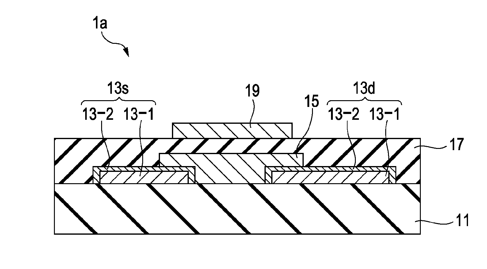
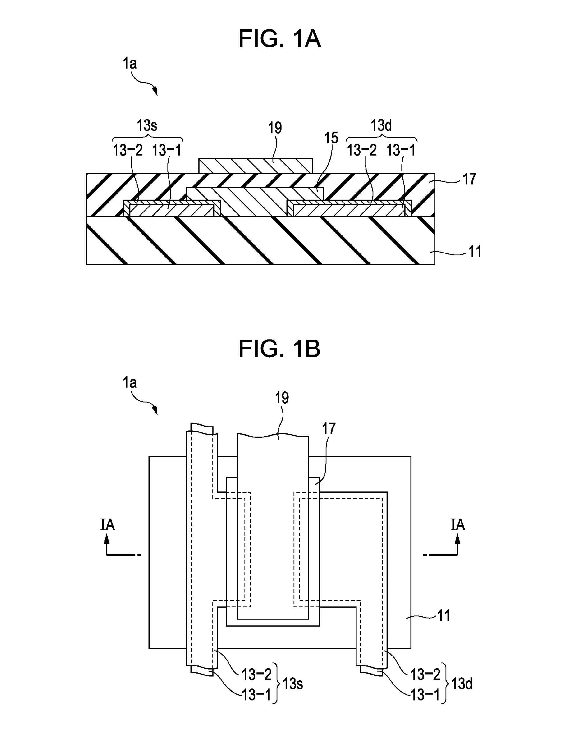
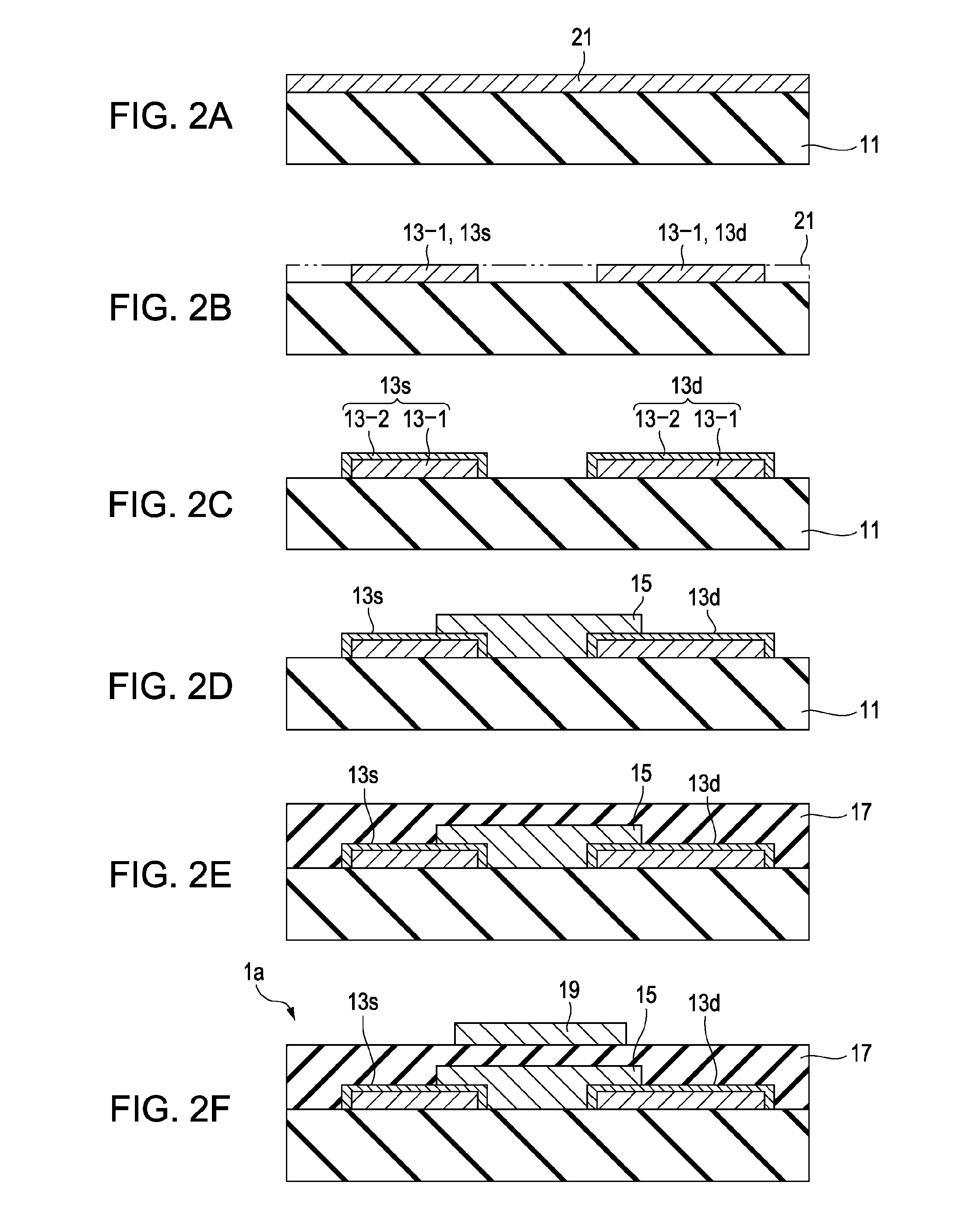
[0027]FIG. 1A is a cross-sectional view of an organic thin film transistor according to a first embodiment and FIG. 1B is a plan view of the organic thin film transistor of the first embodiment. FIG. 1A is the sectional view taken along the line A-A′ of the structure of FIG. 1B.

[0028]An organic thin film transistor 1a shown in these drawings is configured to be a top-gate bottom-contact type thin film transistor, and is provided with a source electrode 13s and a drain electrode 13d, an organic semiconductor layer 15, a gate insulating film 17, and a gate electrode 19, sequentially in that order from the side of a substrate 11. Each of the source electrode 13s and drain electrode 13d is formed, in particular, as a stacked structure formed of a first layer 13-1 and second layer 13-2. There will be explained hereinbelow in detail the structure sequentially from the side of the substrate 11.

[0029]The substrate 11 is formed, including a struct...

second embodiment

Configuration of Organic Thin Film Transistor

[0050]FIG. 3A is a cross-sectional view of an organic thin film transistor according to a second embodiment and FIG. 3B is a plan view of the organic thin film transistor of the second embodiment. FIG. 3A is the sectional view taken along the line A-A′ of the structure of FIG. 3B. The configuration of an organic thin film transistor 1b according to the second embodiment is explained hereinbelow, in which the components similar to those of the organic thin film transistor of the first embodiment described earlier referring to FIGS. 1A and 1B are shown with identical numerical representations.

[0051]The organic thin film transistor 1b shown in FIGS. 3A and 3B is configured to be a bottom-gate bottom-contact type thin film transistor, and is provided with a gate electrode 19, a gate insulating film 17′, a source electrode 13s, a drain electrode 13d, and an organic semiconductor layer 15, sequentially in that order from the side of a substrate...

third embodiment

Configuration of Organic Thin Film Transistor

[0071]FIG. 5 is a cross-sectional view of an organic thin film transistor according to the third embodiment. In addition, a plan view of the organic thin film transistor of this third embodiment is similar to FIG. 3B shown earlier in the second embodiment, and FIG. 5 corresponds to the sectional view taken along the line A-A′ of the structure of FIG. 3B. The configuration of an organic thin film transistor 1c according to the third embodiment is explained hereinbelow, in which the components similar to those of the organic thin film transistor of the second embodiment described earlier in reference to FIGS. 3A and 3B are shown with identical numerical representations.

[0072]The organic thin film transistor 1c shown in FIG. 5 of the third embodiment differs from the organic thin film transistor (1b) of the second embodiment explained in reference to FIGS. 3A and 3B, by the configuration of its source electrode 13s′ and drain electrode 13d′....


PUM

PropertyMeasurementUnit
conductiveaaaaaaaaaa
temperaturesaaaaaaaaaa
flexibleaaaaaaaaaa

Abstract

An organic thin film transistor is disclosed, including a substrate formed of an organic insulating layer, a first layer deposited on the substrate using a plating technique to be used for forming a source electrode and a drain electrode, a second layer of a metal material deposited covering the first layer using a further plating technique to be used for forming the source electrode and the drain electrode with the metal material capable of forming an ohmic contact with an organic semiconductor material lower than the first layer, and an organic semiconductor layer over a region between the source electrode and the drain electrode, which are each formed with the first layer and the second layer. Also disclosed is an electric device provided with the organic thin film transistor.

Description

BACKGROUND OF THE INVENTION[0001]1. Field of the Invention[0002]The present invention relates to an organic thin film transistor, a production method thereof, and an electronic device. More particularly, the invention relates to a bottom-contact type organic thin film transistor formed of a source electrode and drain electrode with an organic semiconductor layer formed thereon, a production method of the organic thin film transistor, and an electronic device provided with the organic thin film transistor.[0003]2. Description of the Related Art[0004]Thin film transistors using an organic semiconductor layer as an active layer, the so-called organic thin film transistors, have been attracting much attention in recent years. Since the organic semiconductor layer as the active layer in the organic thin film transistor can be formed by a film coating method at relatively low temperatures, this is advantageous for reducing production costs, also enables its formation on a flexible, low he...

Claims


Application Information

Patent Timeline
Patent Type & Authority Applications(United States)
IPC IPC(8): H01L51/10H01L51/40
CPCH01L51/0021H01L51/0541H01L51/105H01L51/052H01L51/0545Y02E10/549Y02P70/50H10K71/60H10K10/464H10K10/466H10K77/10H10K10/471H10K10/84
Inventor NOMOTO, KAZUMASAYONEYA, NOBUHIDEOHE, TAKAHIRO
Owner SONY CORP
Why Eureka
Try Eureka