
Electro-optical device and electronic apparatus

a technology of optical devices and electronic devices, applied in the direction of cathode ray tubes/electron beam tubes, instruments, electric discharge tubes, etc., can solve the problems of affecting the quality of display images, etc., to achieve the effect of reducing electronic noise and high quality

Active Publication Date: 2010-02-11
SEIKO EPSON CORP
View PDF3 Cites 26 Cited by
  • Summary
  • Abstract
  • Description
  • Claims
  • Application Information

AI Technical Summary

Benefits of technology

[0007]An advantage of some aspects of the invention is that it provides an electro-optical device capable of displaying an image with a high quality by reducing an electronic noise contained in an image signal and an electronic apparatus including the electro-optical device.

Problems solved by technology

Accordingly, in the respective conductive layers as wirings or electrodes, when voltage such as signal voltage or power voltage is applied to the respective conductive layers or when current such as signal current or power current flows, an electronic noise occurs between the plurality of conductive layers.
In particular, when an image signal in an image signal line is affected by the electronic noise, the image signal may be distorted and the quality of a display image may thus deteriorate.
Therefore, a more serious problem is caused.
However, a basic concept of miniaturization of the electro-optical device may not be realized
Moreover, since an image signal is supplied to every pixel in an active matrix type, a potential difference of course occurs between the pixel electrode in another pixel and the relay wiring.
In consequence, if this problem with the potential difference is not solved, an electric field caused due to the potential difference occurs between the relay wiring and the data line or a conductive layer such as a pixel electrode in another pixel.
Moreover, the electric field cannot be blocked in an area other than the area occupied by the first shield layer.
However, when the electric field is partially blocked by the first shield layer, the electric field can be blocked to a great extent.
Moreover, the electric field cannot be blocked in an area other than the area occupied by the second shield layer.
However, when the electric field is partially blocked by the second shield layer, the electric field can be blocked to a great extent.

Method used


Image

  • Electro-optical device and electronic apparatus
  • Electro-optical device and electronic apparatus
  • Electro-optical device and electronic apparatus

Examples


first embodiment

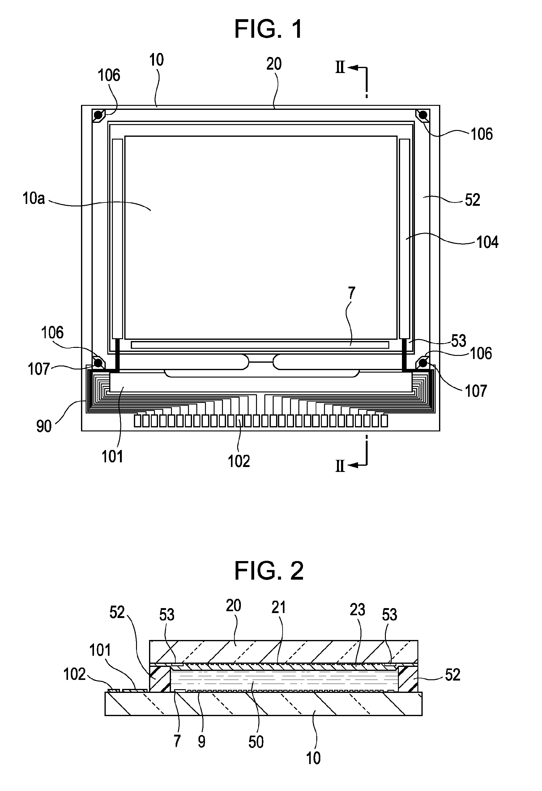
[0044]First, the general structure of a liquid crystal device according to this embodiment will be described with reference to FIGS. 1 and 2. Here, FIG. 1 is a top view illustrating the general structure of the liquid crystal device according to this embodiment. FIG. 2 is a sectional view taken along the line II-II of FIG. 1.

[0045]In FIGS. 1 and 2, the liquid crystal device according to this embodiment includes a TFT array substrate 10 and a counter substrate 20 opposed to each other. The TFT array substrate 10 is a quartz substrate, a transparent substrate such as a glass substrate, or a silicon substrate, for example. The counter substrate 20 is a quartz substrate or a transparent substrate such as a glass substrate, for example. A liquid crystal layer 50 is sealed between the TFT array substrate 10 and the counter substrate 20. The TFT array substrate 10 and the counter substrate 20 is adhered by a sealing member 52 provided in a sealing area located in the circumference of an im...

second embodiment

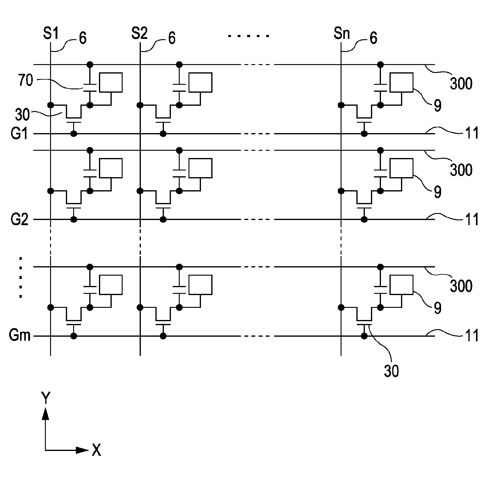
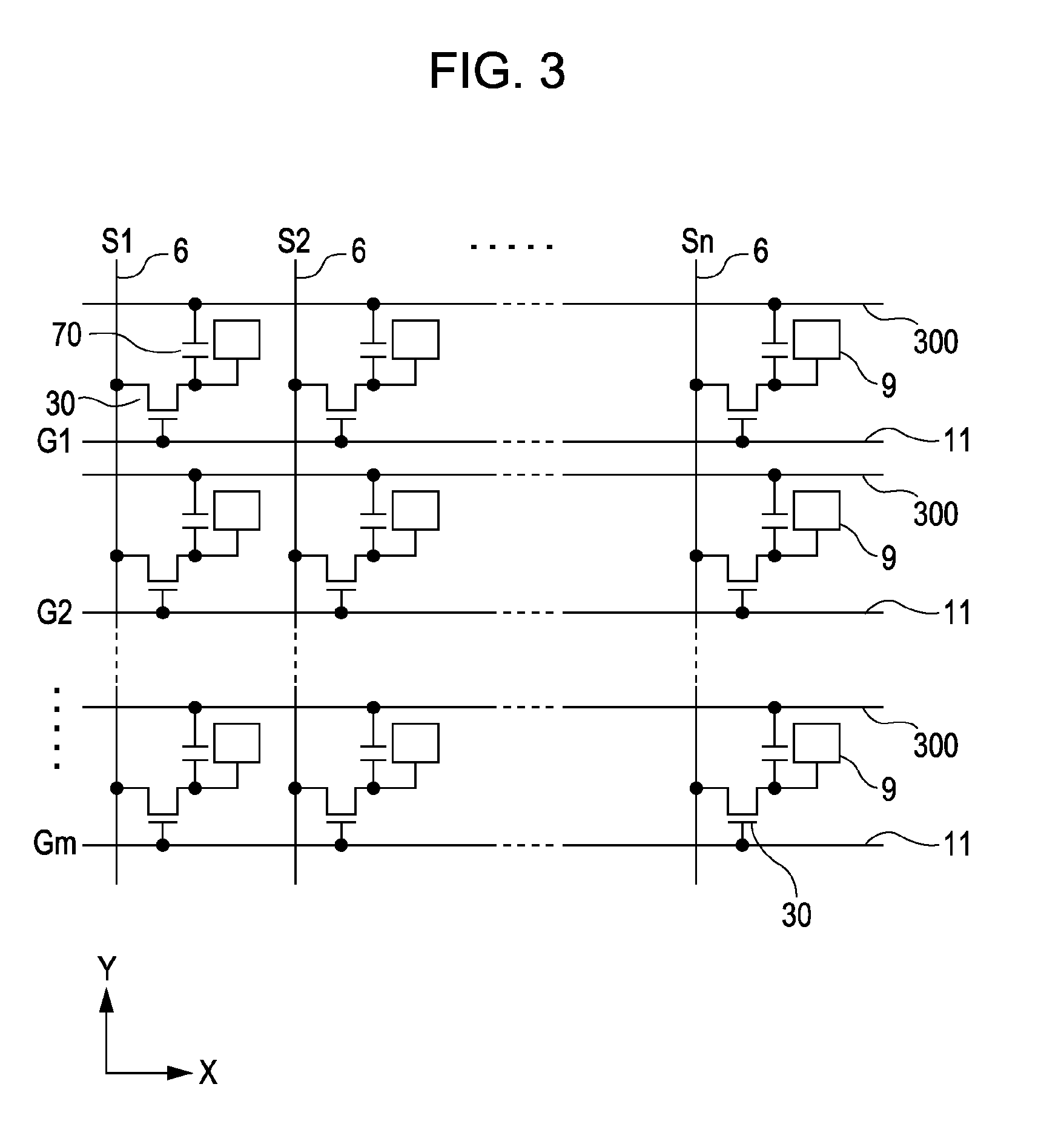
[0076]Next, a second embodiment will be described with reference to FIGS. 7 to 10. The second embodiment is different from the first embodiment in that each storage capacitor 70 (see FIG. 3) is formed by using a second shield layer 5 and a second drain relay wiring 2 as capacitor electrodes.

[0077]FIG. 7 is a top view illustrating the peripheral structure of pixel switching TFTs 30 formed on the TFT array substrate 10 of a liquid crystal device according to the second embodiment. In FIG. 7, respective layers and respective elements are expressed in different scales in order to allow the respective layers and the respective elements to be recognizable. A basic structure is the same as that in the first embodiment (see FIG. 4), but a dielectric film 7 is additionally provided between electrodes of each storage capacitor 70 The thickness of the dielectric film 7 and the areas of the capacitor electrodes (that is, the second drain relay wiring 2 and the second shield layer 5) are adjuste...


PUM


Abstract

An electro-optical device includes a scanning line, a data line which intersects the scanning line, a pixel electrode which is provided at pixel, and a thin film transistor which has a semiconductor layer having a source area electrically connected to the data line and a drain area electrically connected to the pixel electrode, a relay wiring which is laminated between the semiconductor layer and the pixel electrode and connects the drain area to the pixel electrode, a first shield layer which is laminated between the data line and the relay wiring and is held with predetermined potential, and a second shield layer which is laminated between the pixel electrode and the relay wiring and is held with predetermined potential.

Description

BACKGROUND[0001]1. Technical Field[0002]The present invention relates to an electro-optical device such as a liquid crystal device which includes a thin film transistor as a switching element disposed in each of pixels on an element substrate, for example, and an electronic apparatus such as a liquid crystal projector.[0003]2. Related Art[0004]In a liquid crystal device which is an example of the electro-optical device, alignment of an electro-optical material interposed between a pair of substrates is current-controlled by writing an image signal to pixel electrodes in synchronization with an ON / OFF operation of the respective pixel electrodes by TFTs functioning as a switching element. This switching element, a wiring, or the like is formed so as to have a laminated structure on a substrate.[0005]Reduction of black irregularity in an image display unit (that is, improvement in a contrast) or prevention of deterioration in a pixel lifetime was designed by additionally forming a hol...

Claims


Application Information

Patent Timeline
Patent Type & Authority Applications(United States)
IPC IPC(8): G02F1/1368G02F1/1343
CPCG02F1/136213G02F1/136277G02F1/136286H01J29/02G02F2001/136218G02F2203/34H01J17/04G02F2001/13606G02F1/13606G02F1/136218
Inventor NAKAGAWA, MASASHI
Owner SEIKO EPSON CORP
Learn More