Nonvolatile storage device

a storage device and non-volatile technology, applied in the direction of digital storage, semiconductor devices, instruments, etc., can solve the problems of unstable threshold voltage, disadvantageous variation of voltage threshold, leakage current, etc., to prevent the formation of new filaments, stabilize the holding resistance characteristics, and induce stable filaments.

Inactive Publication Date: 2010-02-18
NEC CORP
View PDF5 Cites 9 Cited by
  • Summary
  • Abstract
  • Description
  • Claims
  • Application Information

AI Technical Summary

Benefits of technology

[0011]The present invention has been made to solve these problems. An object of the present invention is to inhibit a change in the number of current paths caused by the filament formed in the resistance variation layer, thus suppressing a possible variation in operating voltage or threshold voltage. Another object of the present invention is to inhibit a leakage current induced by the grain boundary to prevent a possible change in the resistance value of the resistance variation layer while the nonvolatile storage device is off, thus allowing information to be stably stored and preventing an increase in power consumption.
[0030]In the nonvolatile storage device according to the present invention, in a part of the resistance variation layer located on a region in which current flows as a result of dielectric breakdown of the amorphous insulating layer, a current path corresponding to a filament is formed along the region. Thus, during repeated operation of the nonvolatile storage device, formation of a new filament can be prevented, thus allowing a stable filament to be induced. Consequently, held resistance characteristics can be stabilized. As a result, the nonvolatile storage device exhibits stable storage holding characteristics.
[0031]Furthermore, by making the resistance variation layer being a crystalline layer, a leakage current induced by the grain boundary can be inhibited, thus preventing a possible change in the resistance value of the resistance variation layer while the nonvolatile storage device is off. As a result, information can be stably stored, and a possible increase in power consumption can be prevented.

Problems solved by technology

However, the following problems relating to the safety of the device have been found in the related art in Japanese Patent Laid-Open No. 2006-2108882, APPLIED PHYSICS LETTERS, 2006, 88, p.
093509-1 to 093509-3, the problem occurs in which a voltage threshold changing the resistance disadvantageously varies.
It is considered that the threshold voltage becomes unstable because during repeated operation of the device, a new filament is formed in the resistance variation layer or an already formed filament disappears, resulting in preventing a stable filament from being formed in the resistance variation layer.
In this case, even when the storage device is off, that is, even when the filament in the resistance variation layer is disconnected between the electrodes, a leakage current may result from a grain boundary.
Thus, the leakage current may preclude a pre-stored resistance value from being maintained or increase power consumption.

Method used


Image

  • Nonvolatile storage device
  • Nonvolatile storage device
  • Nonvolatile storage device

Examples


embodiment

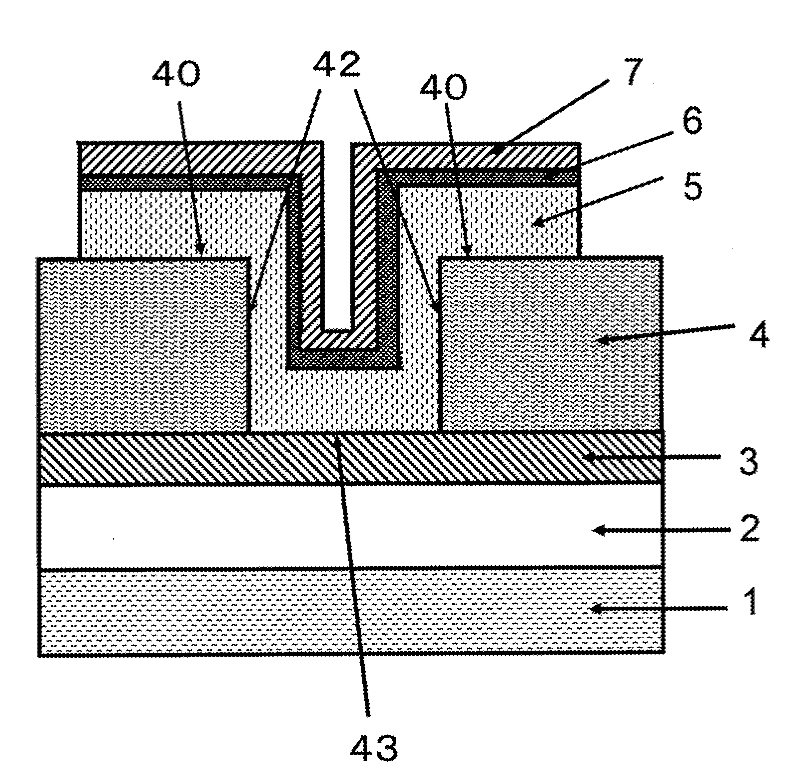
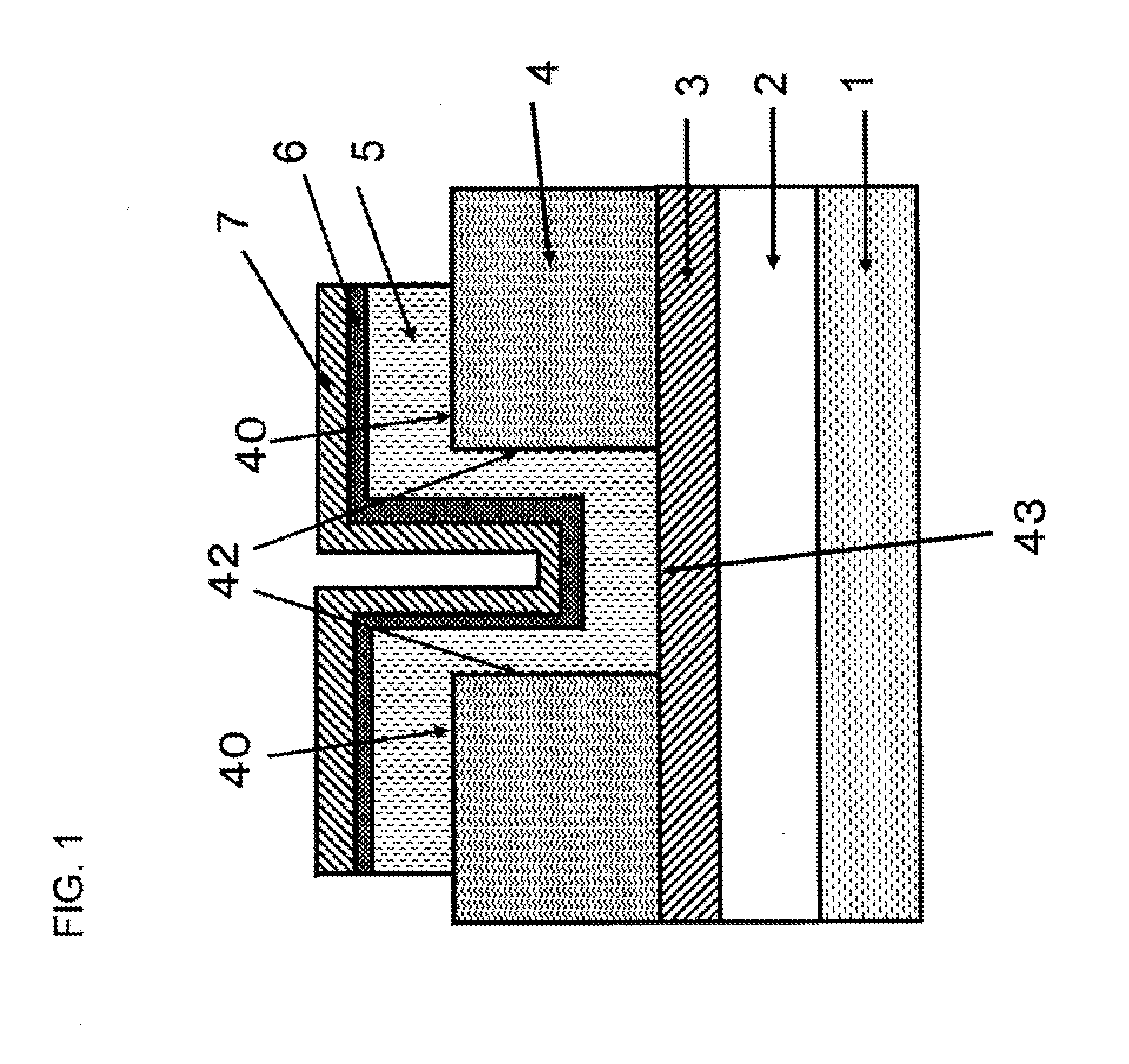
[0072]FIGS. 6 to 9 are sectional views showing a process of producing a nonvolatile storage device according to the present invention. First, the silicon substrate 22 was prepared. The silicon oxide film 23 of film thickness 100 nm was then deposited on the silicon substrate 22 using the CVD method or the thermal oxidation method. Thereafter, the Ti layer 24, TiN layer 25, Ti layer 26 were deposited using the sputtering method. An Ru film of film thickness 100 nm was then deposited. Finally, the lower electrode 27 was formed (FIG. 6(a)).

[0073]Then, the silicon oxide film 28 of film thickness 200 nm was formed using the CVD method (FIG. 6(b)). A photo resist (not shown in the drawings) was deposited so as to cover the silicon oxide film 28. An opening was thereafter formed by photolithography and dry etching (FIG. 7(a)).

[0074]Then, the crystallized nickel oxide (resistance variation layer) 29 was deposited to a film thickness of 10 nm by the sputtering method (FIG. 7(b)). Here, the n...


PUM


Abstract

An element structure for a resistance variable type nonvolatile storage device is provided in which enables a reduction in variation in operating voltage and in a leakage current in an off state of an element. The nonvolatile storage device is characterized by including a lower electrode, an upper electrode, and a laminated structure in which at least one amorphous insulating layer and at least one resistance variation layer are laminated between the lower electrode and the upper electrode.

Description

TECHNICAL FIELD [0001]The present invention relates to a nonvolatile storage device in which the resistance of a resistance variation layer changes between at least two values and in which the change in resistance value is stored as information.BACKGROUND ART [0002]In recent years, nonvolatile storage devices have been actively developed in which stored data does not disappear even when an external power source is turned off. As the nonvolatile storage devices, which now dominate relevant markets, flash memories, MONOSs (Metal Oxide Nitride Oxide Semiconductors), FeRAMs (ferroelectric memories), MRAMs (magnetic storage elements) have been proposed.[0003]However, with miniaturization of memory elements making up each memory cell, ensuring the characteristics of the nonvolatile storage devices as storage elements has been difficult. For example, for the flash memory, a reduction in the thickness of a silicon oxide film between a floating gate (FG) portion and a semiconductor substrate...

Claims


Application Information

Patent Timeline
Patent Type & Authority Applications(United States)
IPC IPC(8): H01L45/00
CPCG11C13/0007G11C2213/32G11C2213/56H01L45/1616H01L45/04H01L45/124H01L45/146H01L27/101H10N70/20H10N70/826H10N70/023H10N70/8833H10N70/8265
Inventor NAKAGAWA, TAKASHI
Owner NEC CORP
Why Eureka
Try Eureka