Display apparatus and drive control method for the same

a technology of drive control and display device, which is applied in the field of display device, can solve the problems of low mobility, affecting the effect of signal transmission, and uneven mobility and achieve the effect of preventing the effect of threshold voltage shift and preventing the error of light emission of light emitting elements due to the application of reverse bias voltag

Active Publication Date: 2010-02-18
SAMSUNG DISPLAY CO LTD
View PDF9 Cites 145 Cited by
  • Summary
  • Abstract
  • Description
  • Claims
  • Application Information

AI Technical Summary

Benefits of technology

[0110]Where a thin film transistor having a current characteristic with a negative threshold voltage is used as the drive transistor, both positive and negative voltages are applied as Vgs at the time of image display, so that the reverse bias voltages have both positive and negative polarities, whereby the reverse bias shortage due to the limited value of reverse bias voltage may be prevented.
[0111]Further, when a common electrode wire is connected to the cathode terminal of the light emitting element to supply different voltages between a reverse bias voltage application period and a period other than the reverse bias voltage application period, erroneous light emission of the light emitting element due to the application of revers...

Problems solved by technology

The low-temperature polysilicon thin film transistor may provide high mobility and stability of threshold voltage, but has a problem that the mobility is not uniform.
The amorphous silicon thin film transistor may provide uniform mobility, but has a problem that the mobility is low and threshold voltage varies with time.
The provision of the compensation circuit described in Patent Document 2, however, causes the pixel circuit to become complicated, resulting in increased cost due to low yield rate and low aperture ratio.
The method described in Patent Document 3 and Patent Document 4, however, can not measure the drive current accurately because the extinction current of an organic EL element of a non-selected pixel circuit gets into the measured drive current.
Further, the method measures a very small drive current for one pixel circuit and has a problem in the measurement accuracy...

Method used


Image

  • Display apparatus and drive control method for the same
  • Display apparatus and drive control method for the same
  • Display apparatus and drive control method for the same

Examples


first embodiment

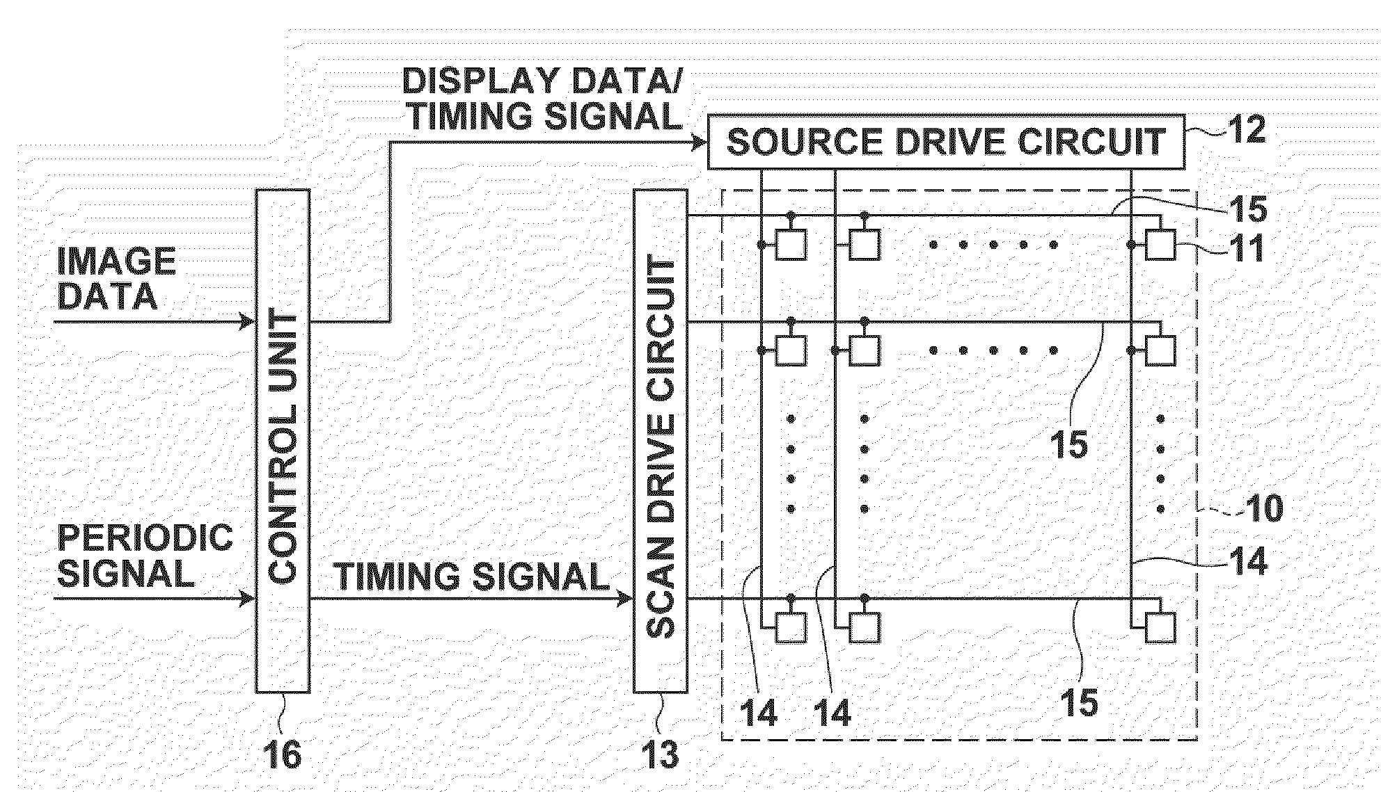
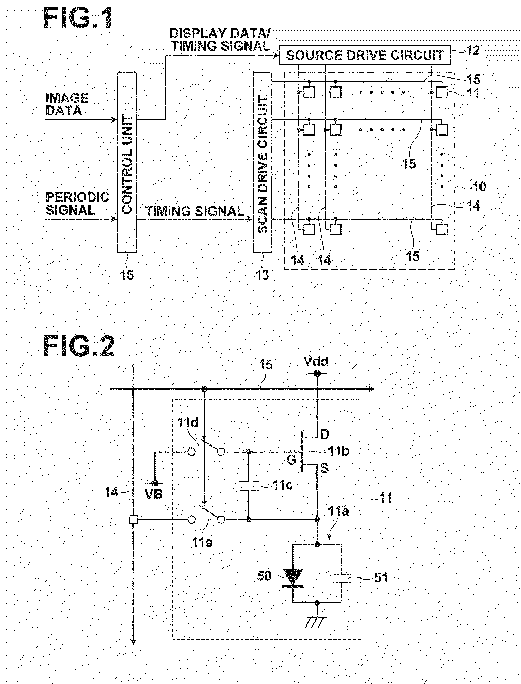
[0133]As illustrated in FIG. 1, the organic EL display device according to the present invention includes active matrix substrate 10 having multiple pixel circuits 11 disposed thereon two-dimensionally, each for holding charges according to a data signal outputted from source drive circuit 12 and applying a drive current through an organic EL element according to the amount of charges held therein, source drive circuit 12 that outputs a data signal to each pixel circuit 11 of the active matrix substrate 10, scan drive circuit 13 that outputs a scan signal to each pixel circuit 11 of the active matrix substrate 10, and control unit 16 that outputs display data according to image data and a timing signal based on a synchronization signal to source drive circuit 12, and outputs a timing signal based on the synchronization signal to scan drive circuit 13.

[0134]Active matrix substrate 10 further includes multiple data lines 14, each for supplying data signal outputted from source drive c...

second embodiment

[0235]Next, an organic EL display device incorporating the display apparatus of the present invention will be described.

[0236]In the organic EL display device according to the first embodiment, first current value Id1 and second current value Id2 are measured with respect to each pixel circuit 11 in each pixel circuit row during the program operation period of each pixel circuit row to calculate characteristic values, thereby eliminating the need to provide a memory for storing characteristic values of all pixel circuits 11. But characteristics of drive transistors 11b do not change all of a sudden, thus it may not be necessarily required to calculate and update characteristic values of all pixel circuits 11 in each pixel circuit row during each program operation period.

[0237]Consequently, in the organic EL display device according to the second embodiment, characteristic values are calculated and updated only for some of pixel circuits 11 in each pixel circuit row during one progra...

third embodiment

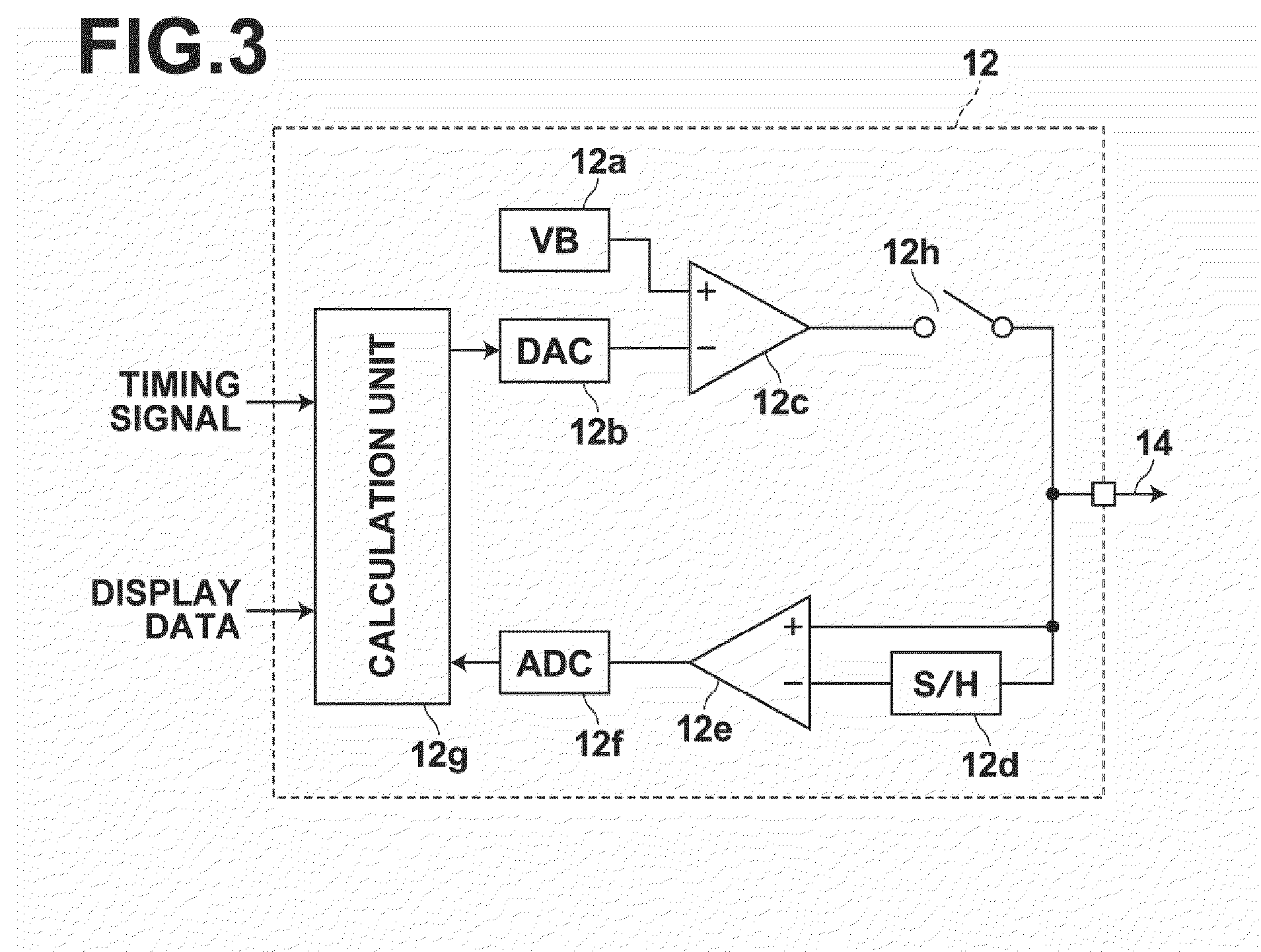
[0318]As illustrated in FIG. 17, source drive circuit 25 of the organic EL display device includes fixed voltage source 25a, D / A converter 25b, first differential amplifier 25c, sample-and-hold circuit 25h, second differential amplifier 25g, A / D converter 25f, calculation unit 25i, first switch element 25j, amplifier 25d, third differential amplifier 25e, and second switch element 25k.

[0319]Fixed voltage source 25a, D / A converter 25b, first differential amplifier 25c, sample-and-hold circuit 25h, second differential amplifier 25g, A / D converter 25f, calculation unit 25i, and first switch element 25j are identical those of the organic EL display device according to the first embodiment.

[0320]Amplifier 25d multiplies display gate-source voltage Vgsn calculated by VGS calculation unit 20k in calculation unit 25i by Kr and outputs the multiplied voltage.

[0321]Third differential amplifier 25e calculates reverse bias voltage Vrv by adding VB to the voltage, Kr×Vgsn, outputted from ampli...


PUM


Abstract

Supplying first and second measuring voltages to a source terminal of a drive transistor to obtain first and second voltage variations at the source terminal of the drive transistor when a parasitic capacitance of a light emitting element is charged by currents flowed through the drive transistor by the supply of the voltages, obtaining first and second current values of the drive current of the drive transistor based on the first and second voltage variations, obtaining characteristic values of the drive transistor based on the first and second measuring voltages and the first and second current values, and outputting a data signal based on the obtained characteristic values and a drive voltage of the drive transistor corresponding to the amount of emission of the light emitting element to the source terminal of the drive transistor.

Description

BACKGROUND OF THE INVENTION[0001]1. Field of the Invention[0002]The present invention relates to a display apparatus having a light emitting element driven by an active matrix method and a drive control method for the display apparatus.[0003]2. Description of the Related Art[0004]Display devices using light emitting elements, such as organic EL elements, for use in various applications, including televisions, cell phone displays, and the like, have been proposed.[0005]Generally, organic EL elements are current driven light emitting elements and, unlike a liquid crystal display, require, as minimum, selection transistors for selecting pixel circuits, holding capacitors for holding charges according to an image to be displayed, and drive transistors for driving the organic EL elements as the drive circuit as described, for example, U.S. Pat. No. 5,684,365 (Patent Document 1).[0006]Heretofore, thin film transistors of low-temperature polysilicon or amorphous silicon have been used in p...

Claims


Application Information

Patent Timeline
IPC IPC(8): G09G5/00
CPCG09G3/3233G09G3/3291G09G2300/0847G09G2360/16G09G2320/0285G09G2320/0295G09G2320/043G09G2300/0866
Inventor SETO, YASUHIRO
Owner SAMSUNG DISPLAY CO LTD
Why Eureka
Try Eureka