Two terminal quantum device using mos capacitor structure

Active Publication Date: 2010-02-25
TEXAS INSTR INC
View PDF4 Cites 6 Cited by
  • Summary
  • Abstract
  • Description
  • Claims
  • Application Information

AI Technical Summary

Benefits of technology

[0004]The instant invention provides a gated quantum well device which is formed in a metal oxide semiconductor (MOS) capacitor structure. An inversion region under the MOS gate forms a quantum well that is preferably less than 20 nanometers wide, causing desirable separation of electron or hole energy levels in the quantum well. The gated quantum well device may be operated as

Problems solved by technology

Integrating quantum well devices in silicon integrated circuits which feature energy level

Method used


Image

  • Two terminal quantum device using mos capacitor structure
  • Two terminal quantum device using mos capacitor structure
  • Two terminal quantum device using mos capacitor structure

Examples


first embodiment

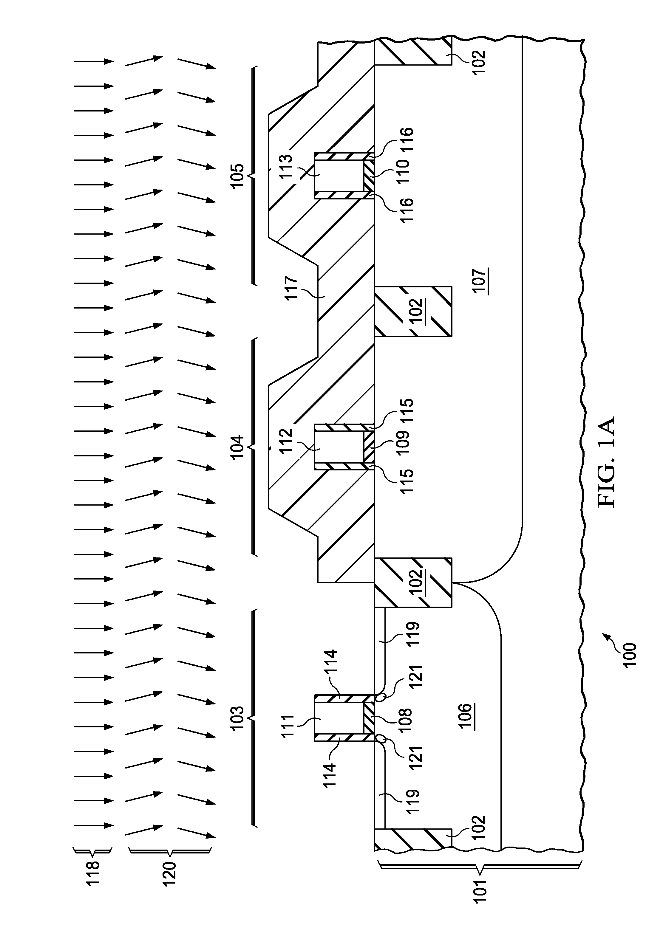
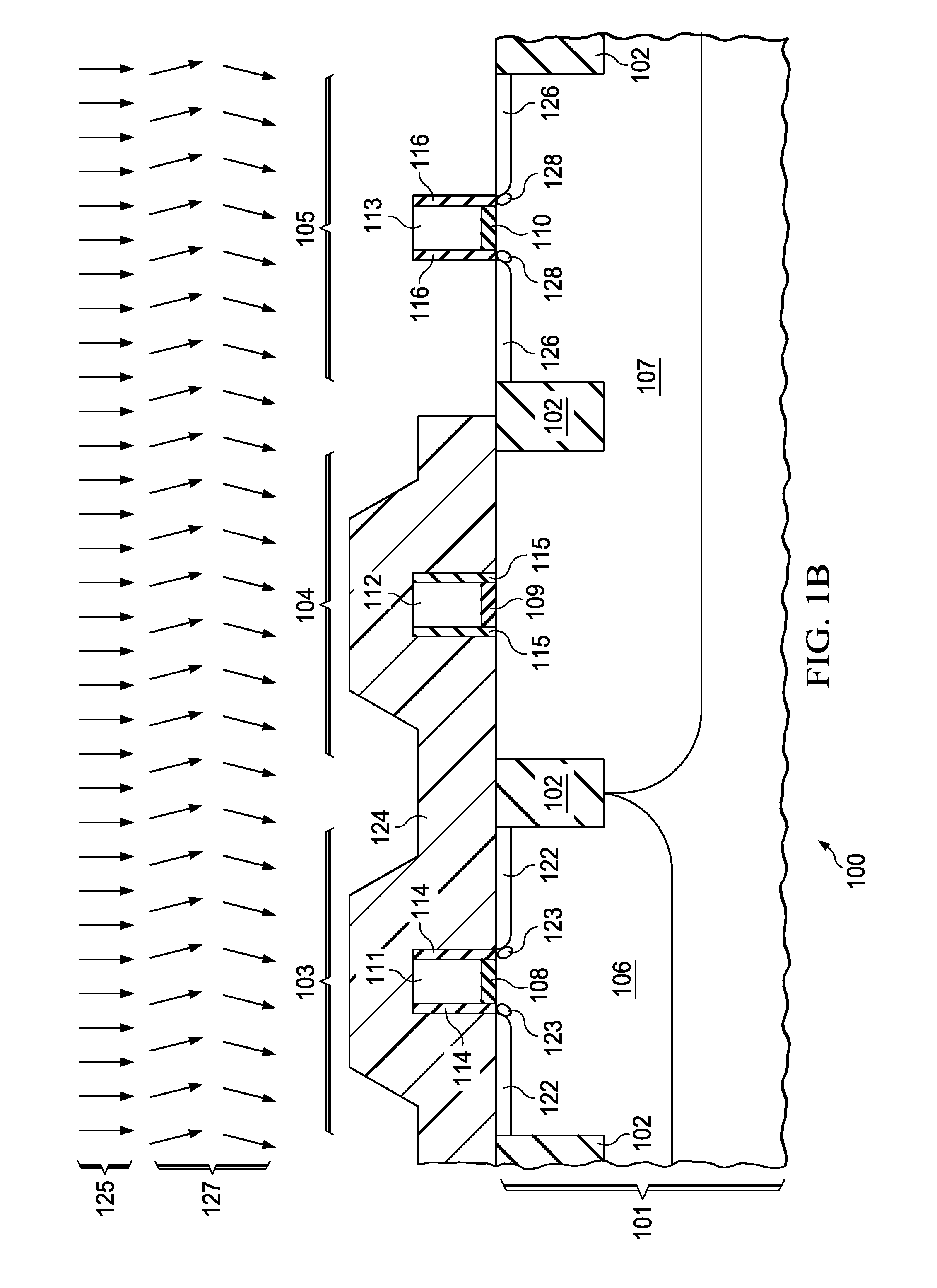
[0019]FIG. 1A through FIG. 1D are cross-sections of a CMOS IC including a gated quantum well device formed according to the instant invention, depicted in successive stages of fabrication. Referring to FIG. 1A, the IC (100) is formed in a semiconductor substrate (101), typically p-type single crystal silicon, but possibly a silicon-on-insulator (SOI) substrate, a hybrid orientation technology (HOT) substrate with regions of silicon or silicon-germanium with different crystal orientations, or any other structure appropriate for fabrication of a CMOS IC. Elements of field oxide (102) are formed by a shallow trench isolation (STI) process sequence, in which trenches, commonly 200 to 500 nanometers deep, are etched into the substrate (101), electrically passivated, commonly by growing a thermal oxide layer on sidewalls of the trenches, and filled with insulating material, typically silicon dioxide, commonly by a high density plasma (HDP) process or an ozone based thermal chemical vapor ...

second embodiment

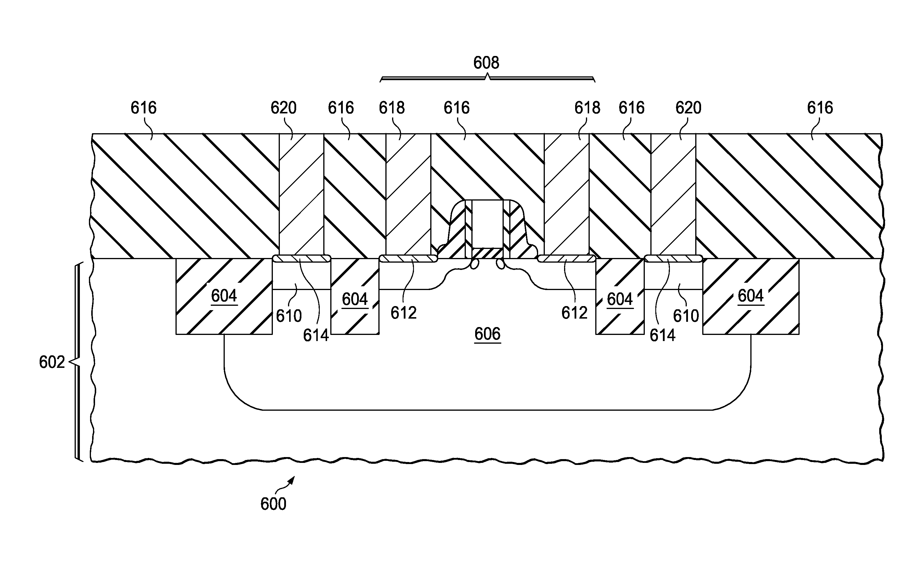
[0036]FIG. 5A through FIG. 5C are cross-sections of a CMOS IC including a gated quantum well device formed according to the instant invention, depicted in successive stages of fabrication. Referring to FIG. 5A, the IC (500) is formed in a semiconductor substrate (501) with the properties described in reference to FIG. 1A. Elements of field oxide (502) are formed in the substrate (501) by an STI process, separating an NMOS region (503), a gated quantum well device region (504) and a PMOS region (505). A p-well (506) is formed in the substrate (501) in the NMOS region (503) and the gated quantum well device region (504) as described in reference to FIG. 1A. Similarly, an n-well (507) is formed in the substrate (501) in the PMOS region (505) as described in reference to FIG. 1A. An NMOS gate dielectric layer (508), a gated quantum well device gate dielectric layer (509) and a PMOS gate dielectric layer (510) are formed on top surfaces of the substrate (501), with the properties describ...


PUM


Abstract

A gated quantum well device formed as an MOS capacitor is disclosed. The quantum well is an inversion region less than 20 nanometers wide under the MOS gate. The device may be fabricated in either polarity, and integrated into a CMOS IC, configured as a quantum dot device or a quantum wire device. The device may be operated as a precision charge pump, with a minority carrier injection region added to speed well filling.

Description

FIELD OF THE INVENTION[0001]This invention relates to the field of integrated circuits. More particularly, this invention relates to gated quantum well devices in integrated circuits.BACKGROUND OF THE INVENTION[0002]Charge pumps based on quantum wells offer advantages over conventional charge pumps based on MOS transistors, including delivery of precise quantities of charge. Integrating quantum well devices in silicon integrated circuits which feature energy level separations greater than 50 meV to allow operation at room temperature has been problematic.SUMMARY OF THE INVENTION[0003]This Summary is provided to comply with 37 C.F.R. §1.73, requiring a summary of the invention briefly indicating the nature and substance of the invention. It is submitted with the understanding that it will not be used to interpret or limit the scope or meaning of the claims.[0004]The instant invention provides a gated quantum well device which is formed in a metal oxide semiconductor (MOS) capacitor s...

Claims


Application Information

Patent Timeline
IPC IPC(8): G05F1/10H01L29/66H01L21/336
CPCH01L29/94
Inventor CHATTERJEE, TATHAGATAEDWARDS, HENRY LITZMANNBOWEN, CHRIS
Owner TEXAS INSTR INC
Why Eureka
Try Eureka