Gas sensor made of field effect transistor based on ZnO nanowires

a field effect transistor and nanowire technology, applied in the field of gas sensor devices, can solve the problems of small gate voltage variation, urgent study and manufacturing of gas sensor devices for various gases, and affect the electric current between source and drain, etc., to achieve the effect of small size, large specific surface area, and small siz

Inactive Publication Date: 2010-03-04
NAT FORMOSA UNIV
View PDF2 Cites 30 Cited by
  • Summary
  • Abstract
  • Description
  • Claims
  • Application Information

AI Technical Summary

Benefits of technology

[0039]The ZnO nanowire FET gas sensor device disclosed in the present invention has a small size and is essentially an electronic device like MOSFET. Except for Si substrate, the metal, insulator, and semiconductor are thin films from nanometer to micrometer in thickness. The ZnO nanowire can used the gas sensing material and the charge carrier channel. The ZnO nanowire is an n-type semiconductor itself and has a large specific surface area. Therefore, the gas sensor device made from ZnO nanowire FET disclosed in the present invention has the advantages as follows: (1) small size, light weight, and little material needed; (2) low manufacturing cost due to the utilization of the known semiconductor technology; and (3) high performance for sensing gas.

Problems solved by technology

Therefore, the studying and manufacturing of the gas sensor device for various gases are needed and urgent [1].
In other words, a small variation of gate voltage can much affect the electric current between source and drain.

Method used


Image

  • Gas sensor made of field effect transistor based on ZnO nanowires
  • Gas sensor made of field effect transistor based on ZnO nanowires
  • Gas sensor made of field effect transistor based on ZnO nanowires

Examples


Embodiment Construction

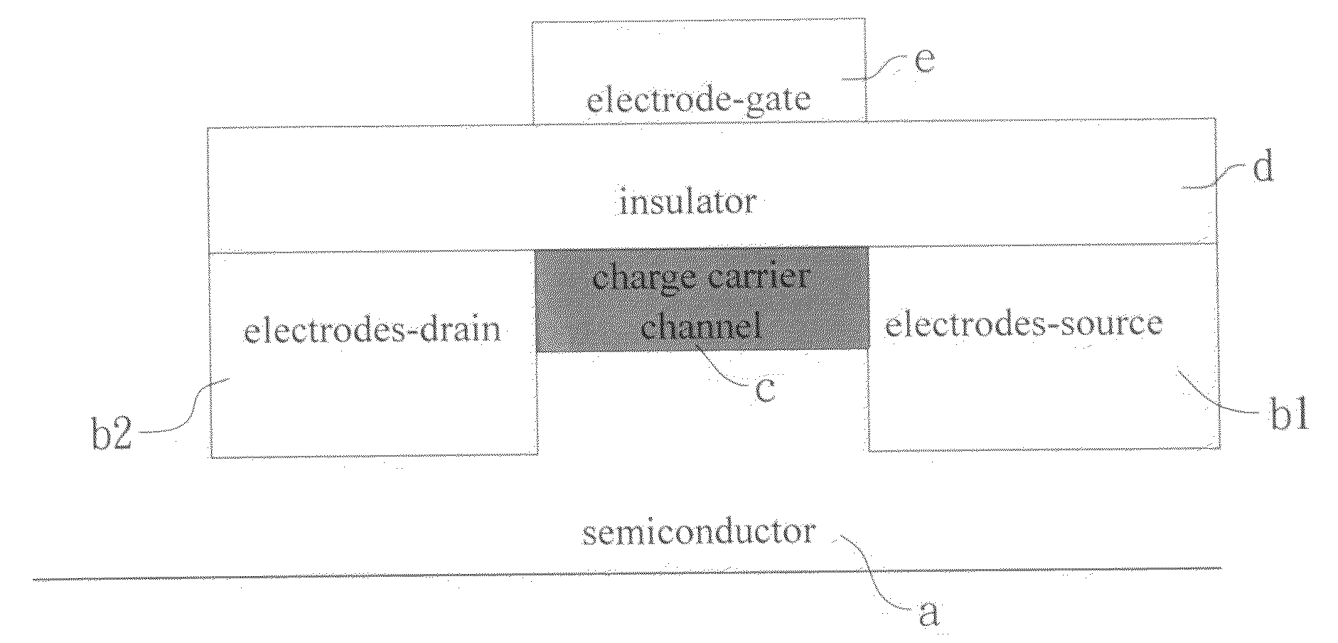
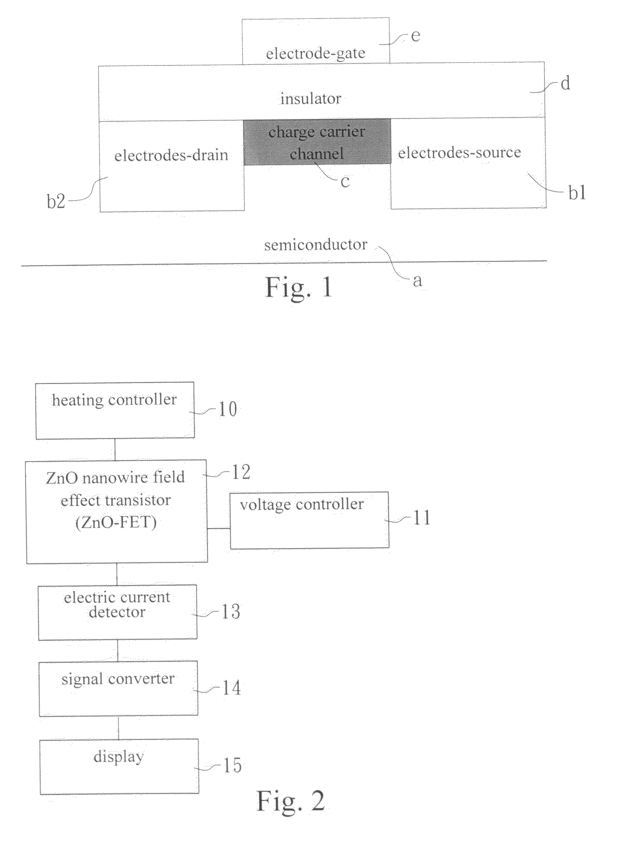
[0050]The gas sensor device made of ZnO nanowire field effect transistor (ZnO-FET) disclosed in the present invention and its peripheric equipments are show in FIG. 2. The peripheric equipments needed in the present invention contains heating controller (10), voltage controller (11), electric current detector (13), signal converter (14), and display (15). These peripheric equipments are the known devices so they do not belong to the claims of the present invention. Here only briefly state their function, and the statement about their structure is then omitted.

[0051]The heating controller (10) is used for heating the ZnO-FET and keeping the ZnO-FET at constant temperature. The heating controller (10) consists of an power supply, a thermometer, and an auto-thermo controller. The voltage controller (11) is used for controlling the voltages of gate, source, and drain. The electric current detector (13) is used to detect the current flowing between source and drain of ZnO-FET. The signal...


PUM

PropertyMeasurementUnit
thicknessaaaaaaaaaa
thicknessaaaaaaaaaa
thicknessaaaaaaaaaa

Abstract

The present invention discloses a gas sensor made of field effect transistor based on ZnO nanowires (ZnO-FET) which operates according to the principle of metal-oxide-semiconductor field effect transistor (MOSFET) and has a charge carrier channel made of ZnO nanowires between source and drain. The gas sensor device disclosed in the present invention has three electrodes-gate, source and drain, so that it is different from the known gas sensor device which has only two electrodes-cathode and anode. The ZnO nanowires as charge channel in the gas sensor device of the present invention is an n-type semiconductor with high specific surface area, and its electric resistance can be controlled by the gate bias, so that the capability of the present device for sensing gas can be largely promoted.

Description

FIELD OF THE INVENTION[0001]The present invention relates to a gas sensor device, especially to a gas sensor device based on the principle of field effect transistor. The gas sensor device has three electrodes:source, drain, and gate, and charge channel made of ZnO nanowires between source and drain. Due to the high specific surface area and the gate bias controlling for the electric resistance of ZnO nanowires, the gas sensor device disclosed in the present invention is superior to the known device in sensing gas.DESCRIPTION OF THE PRIOR ART [0002]There are more and more gases with flammability, explosibility, toxicity created in the human living space along with the science progress and technology development. In order to reduce the environmental contamination and promote the safety of human life, it is necessary to detect and control these harmful gases. Therefore, the studying and manufacturing of the gas sensor device for various gases are needed and urgent [1].[0003]Among the ...

Claims


Application Information

Patent Timeline
Patent Type & Authority Applications(United States)
IPC IPC(8): G01N7/00
CPCG01N27/4141
Inventor LIU, WEI-LONGCHEN, WEN-JAUHHSIEH, SHU-HUEI
Owner NAT FORMOSA UNIV
Why Eureka
Try Eureka