Method to convert waste silicon to high purity silicon

a technology of waste silicon and high purity, applied in the direction of halogenated silane, silicon compounds, manufacturing tools, etc., can solve the problems of low purity (98%-99%) of materials, high energy consumption, and waste of resources, and achieve high purity polysilicon at competitive costs, industrially practical and cost-effective, and robust

Inactive Publication Date: 2010-03-11
HARIHARAN ALLEPPEY V +1
View PDF21 Cites 25 Cited by
  • Summary
  • Abstract
  • Description
  • Claims
  • Application Information

AI Technical Summary

Benefits of technology

[0028]Methods are disclosed to recover silicon from silicon-containing solids recovered from a silicon manufacturing process, and produce high purity polysilicon at competitive costs. Methods are disclosed to provide robust, industrially practical and cost-effective methodology to convert recovered silicon into high purity polysilicon.
[0032]In one or more embodiments, the recovered silicon-containing solids are pretreated prior to converting into gaseous silicon forms to reduce impurities content of the silicon-containing solids.

Problems solved by technology

The processes, collectively called the Siemens Process, are very energy intensive.
This MG-Si material is inexpensive but is of very low (98% -99%) purity.
These residual impurities in MG-Si make it unsuitable for direct use as feedstock for the electronic and PV industries.
These distillation purifications of the TCS contribute to more than 50% of the TCS plant operating costs.
These saw processes also produce significant silicon waste, known as kerf silicon waste, due to the cutting of the silicon ingot or block.
Slicing silicon ingot or block to make wafers is one of the most expensive and wasteful process steps in the silicon value chain, especially in the PV cell manufacturing industry.
This adds significantly to the silicon shortage of the PV industry and in addition, to PV cell manufacturing costs.
While the silicon wafer industry, in collaboration with the wire saw manufacturers, has developed practical processes to recover the cutting fluid and bulk of silicon carbide abrasive from the wafer cutting systems, recovering the silicon powder from the slurry has eluded the PV feedstock industry.
Silicon is also lost in ingot shaping operations and due to lapping and other chemical mechanical operations on wafers.
No serious attempts have been made to recover the silicon powder from these waste streams.
It is very doubtful that such methods will produce high purity PV grade silicon at reasonable cost.
This powder is of high purity, but cannot easily be recycled or used in silicon melting and crystal growth applications because of the finity of the powder.
While the polysilicon industry sometimes practices a simple melting process to recover the silicon dust waste, this process is ineffective, costly and inherently lacks purification of the material.
As with the kerf silicon, the challenge is recovering the silicon dust waste and produce silicon of the correct or improved purity and process cost.

Method used


Image

  • Method to convert waste silicon to high purity silicon
  • Method to convert waste silicon to high purity silicon
  • Method to convert waste silicon to high purity silicon

Examples


Embodiment Construction

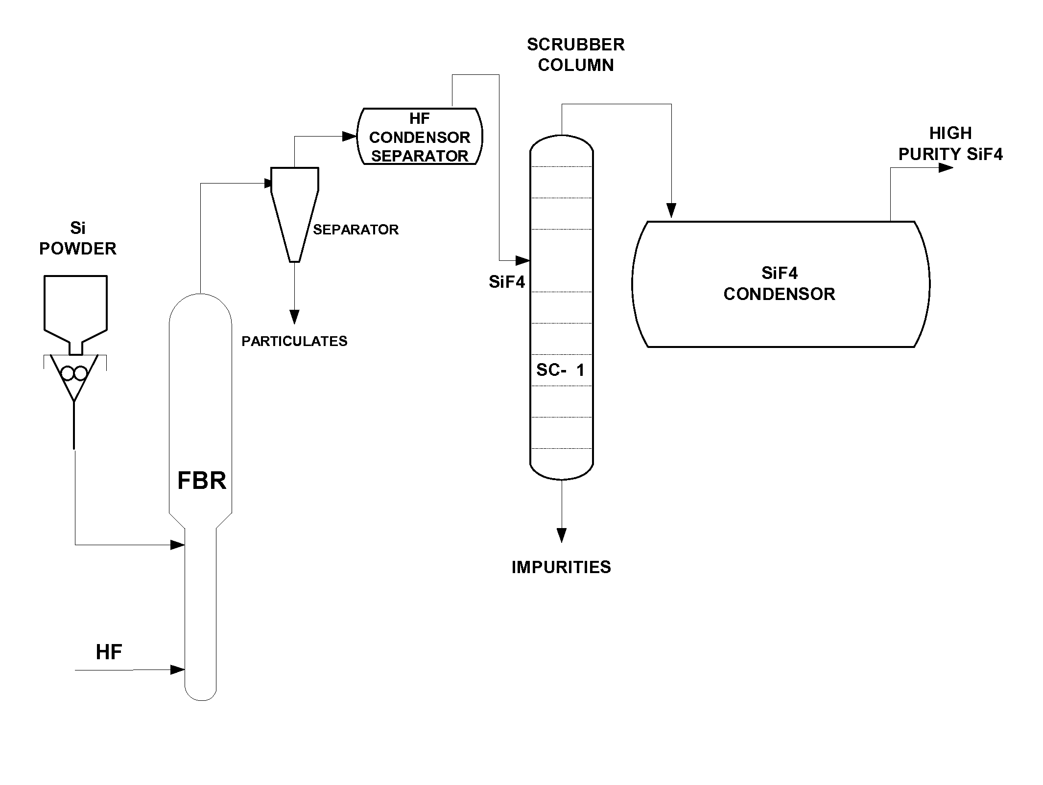
[0079]A process for the recovery of silicon from a silicon fabrication or manufacturing process is described that provides silicon of a desired purity with minimal to low post-recovery purification. The method includes providing high purity silicon solids from a silicon manufacturing process, the silicon solids being substantially free of semiconductor dopants; converting the silicon solids into gaseous silicon forms; and collecting the gaseous silicon forms as a condensed liquid of a silicon-containing compound. The conversion step to gaseous silicon forms substantially removes impurities admixed with silicon in the waste from the fabrication or manufacturing process. The gaseous silicon forms may be used appropriately or eventually converted to polysilicon. The silicon can be of a purity suitable for solar [e.g., >99.999 wt % Si] or electronic [e.g., >99.99999 wt % Si] applications.

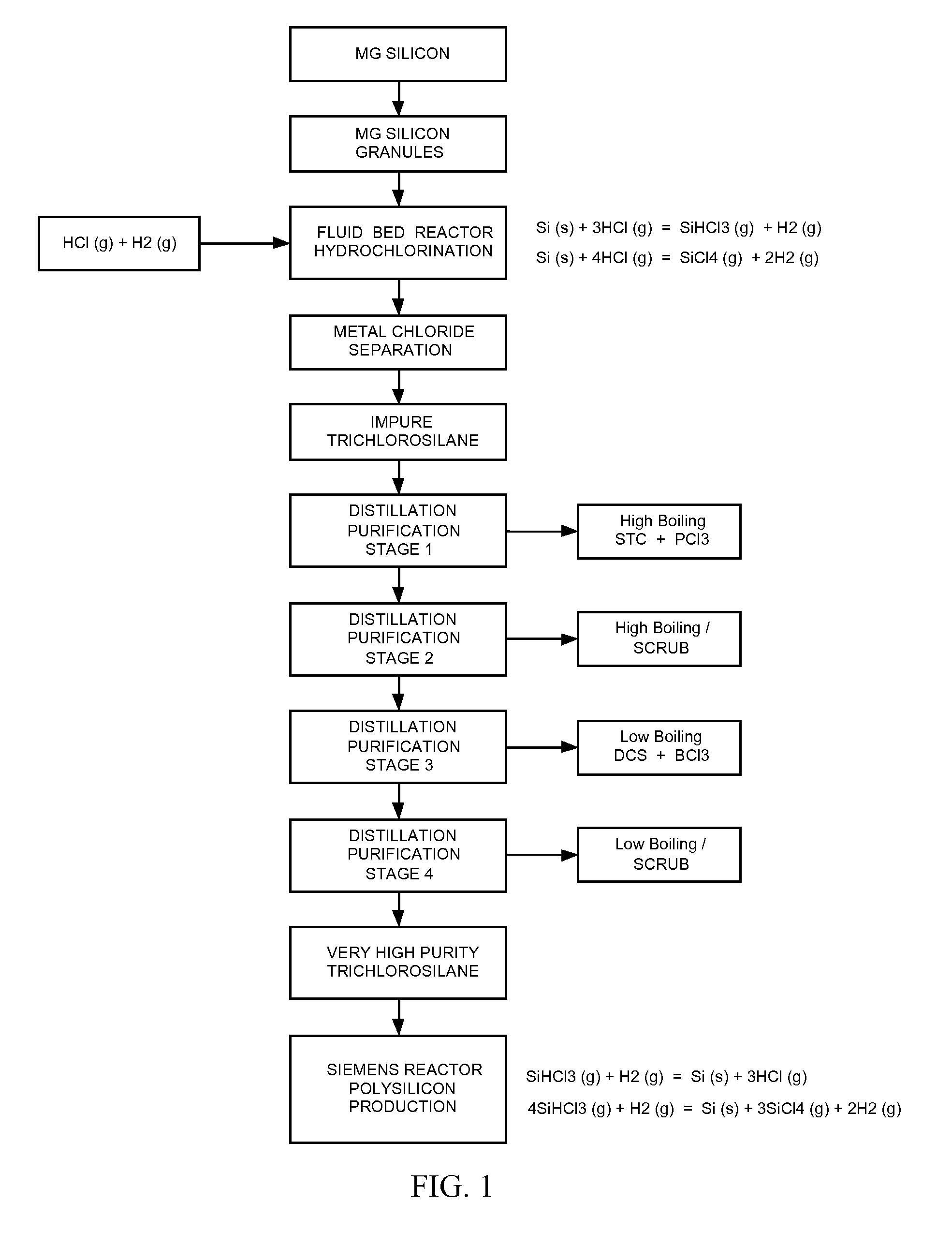
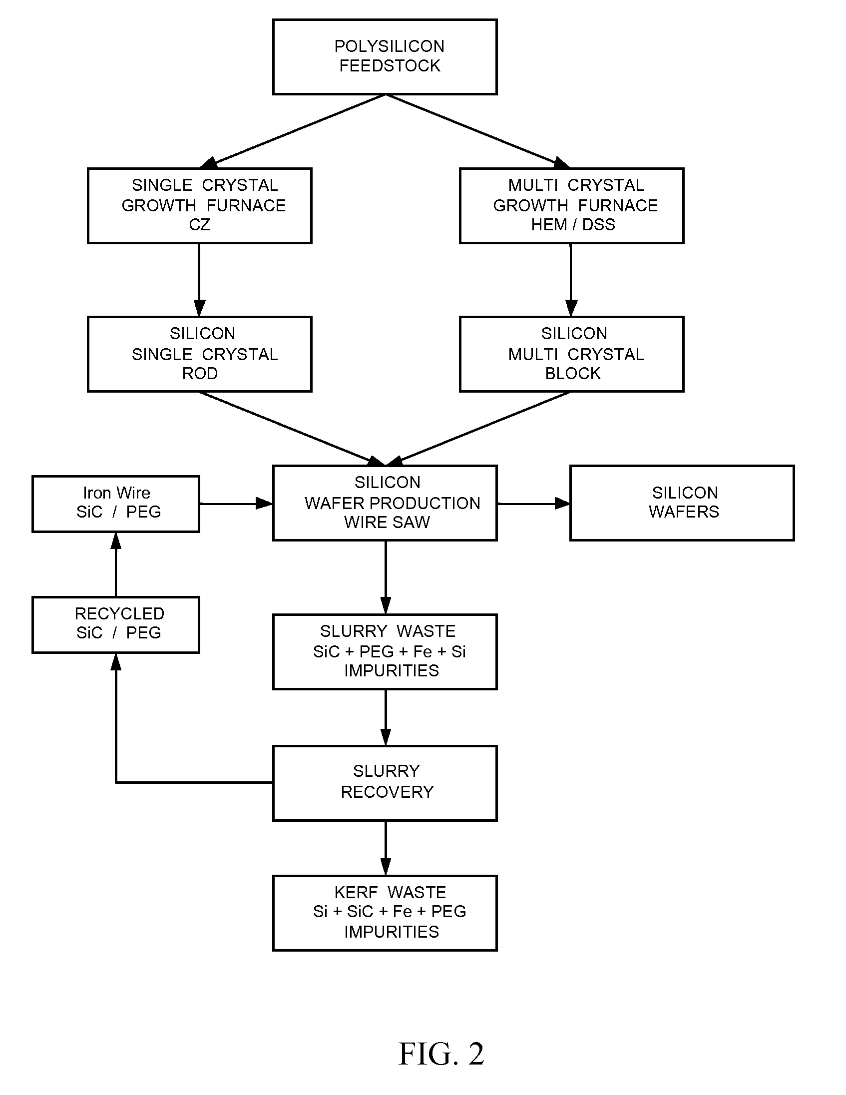
[0080]Silicon manufacturing processes generate huge amounts of silicon powder waste, which can be re...


PUM

PropertyMeasurementUnit
mean particle sizeaaaaaaaaaa
semiconductoraaaaaaaaaa
volatileaaaaaaaaaa

Abstract

A process for the recovery of silicon includes providing silicon-containing solids recovered from a silicon manufacturing process, said recovered silicon-containing solids being substantially free of semiconductor dopants; converting the recovered silicon-containing solids into gaseous silicon forms; subjecting to purification by minimal distillation; collecting the gaseous silicon forms as a condensed liquid of silicon-containing compounds; and utilizing the silicon-containing compounds for silicon deposition.

Description

CROSS-REFERENCE TO RELATED APPLICATIONS[0001]This application claims the benefit of priority under 35 U.S.C. §119(e) to co-pending U.S. Patent Application No. 61 / 137,904 filed on Aug. 4, 2008, entitled “METHOD TO CONVERT KERF SILICON TO HIGH PURITY POLYSILICON,” which is incorporated herein by reference in its entirety.[0002]This application claims the benefit of priority under 35 U.S.C. §119(e) to co-pending U.S. Patent Application No. 61 / 197,714 filed on Oct. 30, 2008, entitled “METHOD TO CONVERT SILICON POWDER TO HIGH PURITY POLYSILICON THROUGH INTERMEDIATE SiF4,” which is incorporated herein by reference in its entirety.[0003]This application claims the benefit of priority under 35 U.S.C. §119(e) to co-pending U.S. Patent Application No. 61 / 210,197 filed on Mar. 16, 2009, entitled “RECOVERY OF SILICON FROM WIRE SAW KERF WASTE,” which is incorporated herein by reference in its entirety.[0004]This application claims the benefit of priority under 35 U.S.C. §119(e) to co-pending U.S...

Claims


Application Information

Patent Timeline
Patent Type & Authority Applications(United States)
IPC IPC(8): C01B33/107C01B33/08C01B33/021
CPCB28D5/007C01B33/021C01B33/037C01B33/10736C01B33/107C01B33/10705C01B33/04Y02P70/10
Inventor HARIHARAN, ALLEPPEY V.RAVI, JAGANNATHAN
Owner HARIHARAN ALLEPPEY V
Why Eureka
Try Eureka