Optical scanning mirror, semiconductor structure and manufacturing method thereof

Inactive Publication Date: 2010-03-18
PANASONIC CORP
View PDF4 Cites 11 Cited by
  • Summary
  • Abstract
  • Description
  • Claims
  • Application Information

AI Technical Summary

Benefits of technology

[0009]The present invention is conceived to consider the above mentioned problems, and purposes to provide an optical scanning mirror which enables to form an insulation structure in a moving unit by simple manufacturing processes, to increase yield ratio of products, to increase resonance frequency of the moving unit without upsizing the device, to increase break-proof and to be easy to use, and a semiconductor structure which is used for the optical scanning mirror and so on.
[0012]According to such configurations, since the supporting member is formed just below the isolation trench and the moving unit is configured to be rotatable integrally with the supporting member, the semiconductor structure can be manufactured by simple manufacturing processes rather than the conventional processes, and mechanical strength of the moving unit can be secured. Furthermore, since the isolation trench are configured to divide the moving unit into a plurality of the regions, it is possible to maintain the electric insulation between the regions surely, and thus, yield ration of the semiconductor structures or the optical scanning mirrors in manufacture can be increased. Furthermore, since the moving unit may not be inclined so much due to the supporting member contacts a mounting face, braking of the hinges can be prevented and the semiconductor structure or the optical scanning mirror can be handled easier. Since the supporting member rotates integrally with the moving unit, resonance frequency of the moving unit can be decreased without upsizing the device, and thus, manufacturing cost of the semiconductor structure or the optical scanning mirror can be decreased.
[0014]According to such manufacturing processes, it is possible to manufacture the semiconductor structure easily by simple processes for etching the SOI substrate, without performing the trench side wall oxidation process, the polysilicon filling process, and the polysilicon polishing process. Since the isolation trench are formed to divide the moving unit into a plurality of regions, electric insulation can be maintained surely between the regions, and thus, yield ration of products in manufacturing of the semiconductor structure can be increased.

Problems solved by technology

However, the manufacturing processes of the semiconductor structure become complicated when the isolation trench 89, which are formed by filling the polysilicon 89a into the trench 801a, is provided to form the movable frame 83.
In addition, since it is difficult to maintain favorite electric insulation and to maintain mechanical strength due to providing the isolation trench 89, simultaneously, there is a problem that yield ratio of the products may be deteriorated.
Furthermore, in the polysilicon filling process, it is difficult to fill the polysilicon 89a thickly into the trenches 801a, so that air gaps may occur in the filled polysilicon 89a, and thus, the mechanical strength of the movable frame 83 may be weaken.
However, since the mirror unit 82 and the movable frame 83 have substantially the same thickness in the conventional structure, it is necessary to upsize the movable frame in order to increase a ratio of the resonance frequencies of the mirror unit 82 and the movable frame 83, and thus, dimensions of the device of the optical scanning mirror 81 will be upsized and manufacturing cost thereof increases.

Method used


Image

  • Optical scanning mirror, semiconductor structure and manufacturing method thereof
  • Optical scanning mirror, semiconductor structure and manufacturing method thereof
  • Optical scanning mirror, semiconductor structure and manufacturing method thereof

Examples


first embodiment

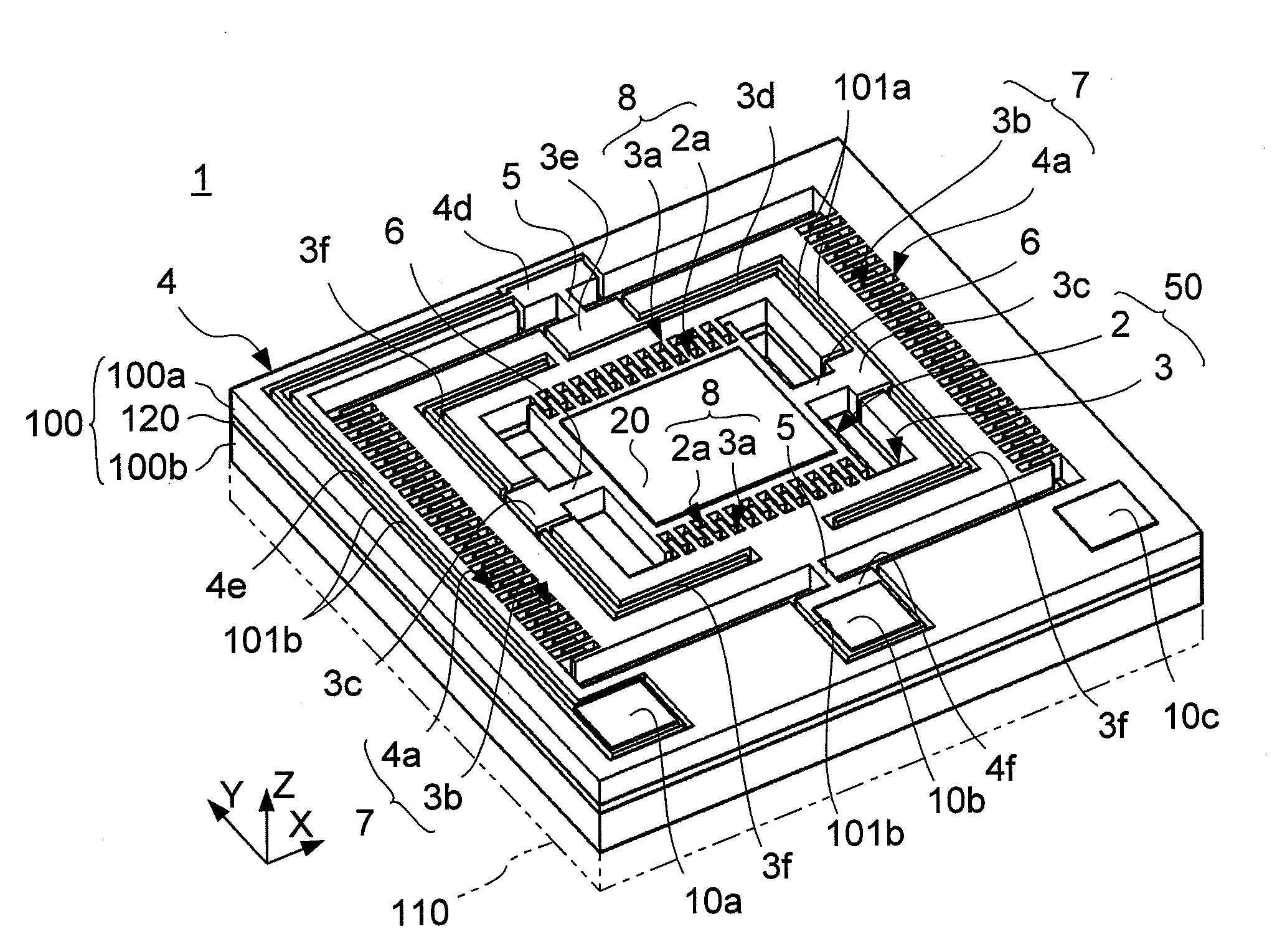
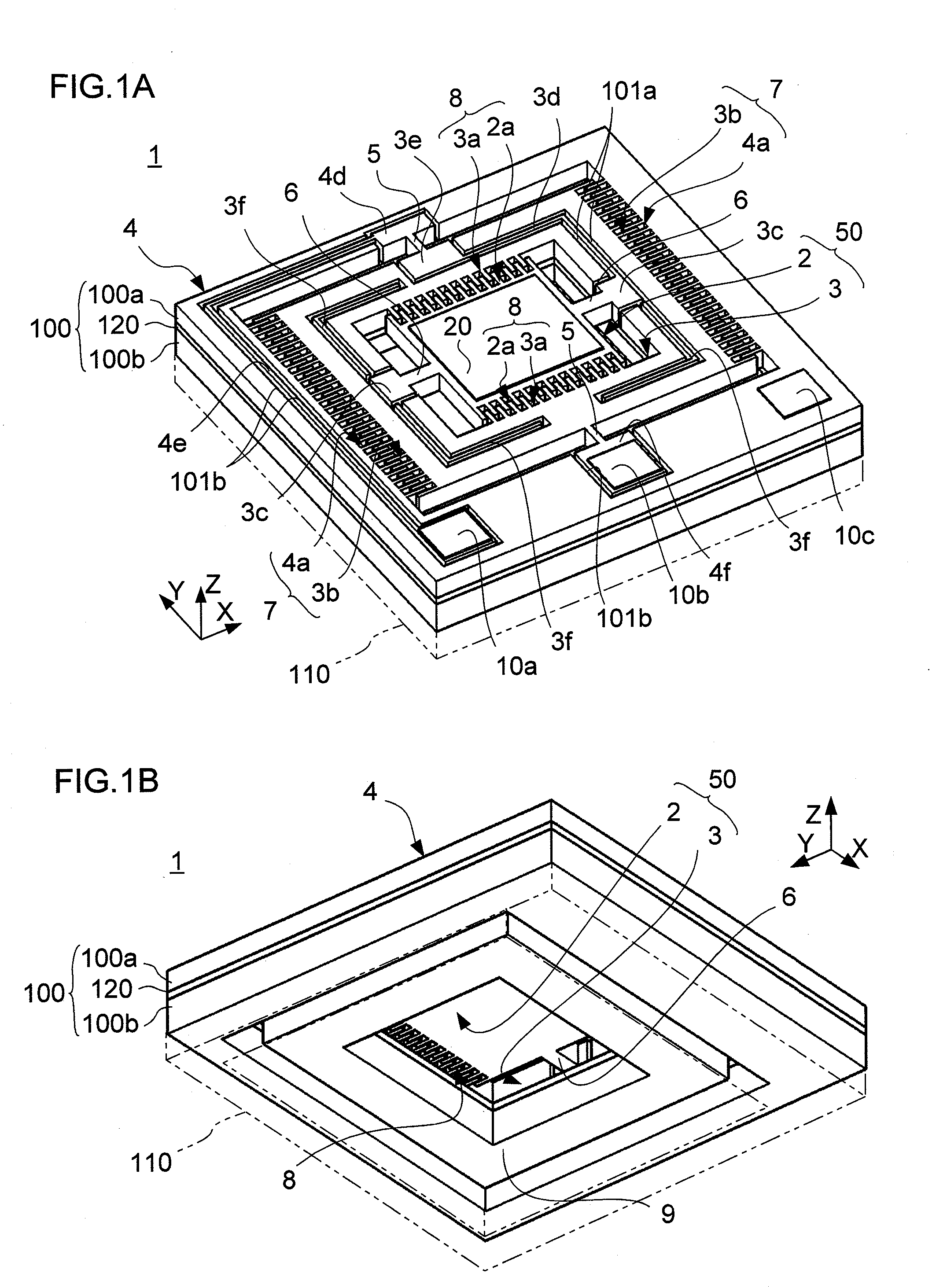
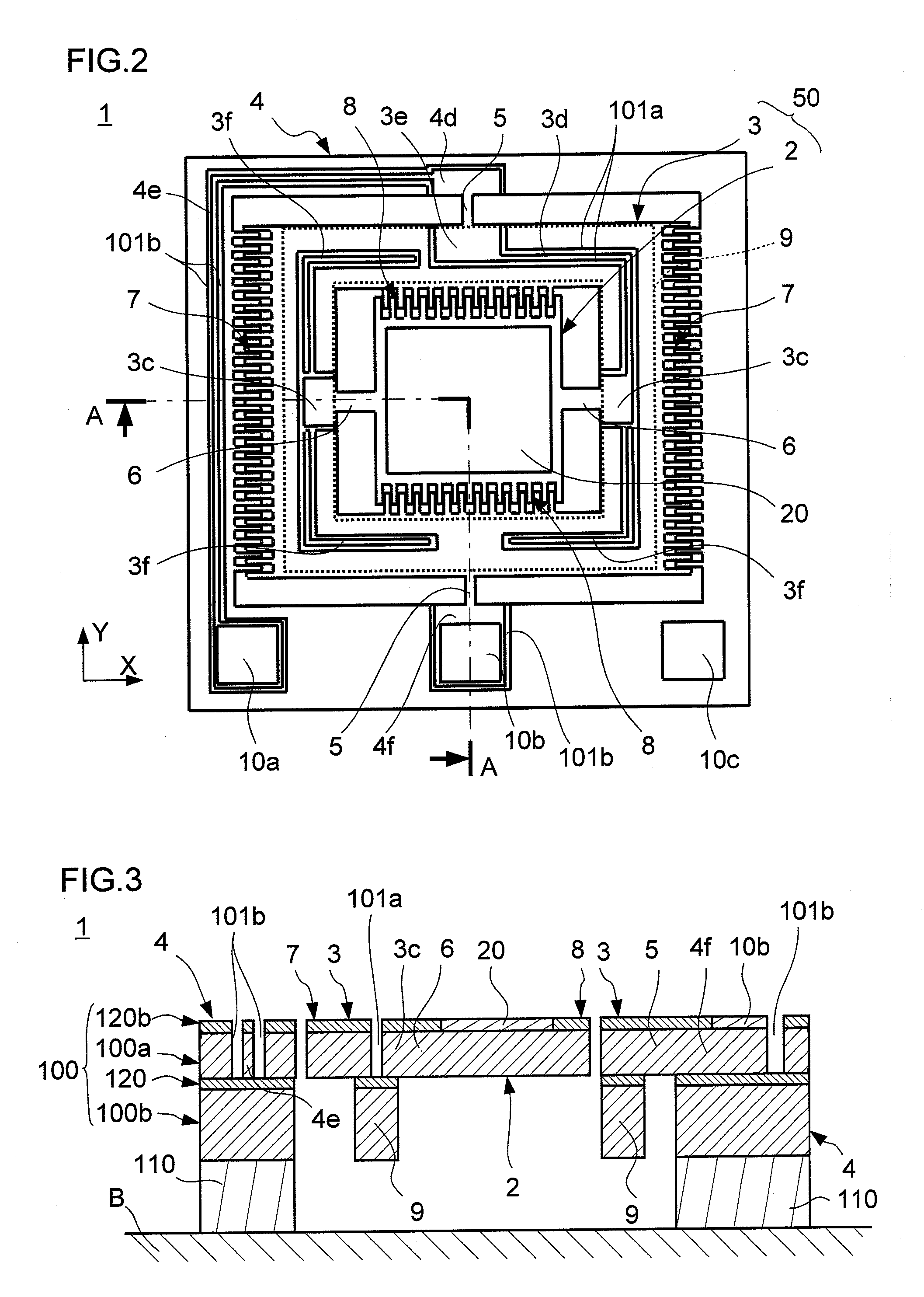
[0042]the present invention is described below with reference to figures. FIG. 1A, FIG. 1B, FIG. 2, FIG. 3, FIG. 4A, FIG. 4B and FIG. 5 show an example of an optical scanning mirror in accordance with in this embodiment. The optical scanning mirror (semiconductor structure) 1 is configured to use a semiconductor structure. The optical scanning mirror 1 is a compact type one equipped in optical equipment such as a bar code reader, a projector apparatus reflecting pictorial image on an external screening or the like, or an optical switch, for example. The optical scanning mirror 1 has a function to scan light beams incoming from external light source (not illustrated).

[0043]First, a configuration of this optical scanning mirror 1 is described. The optical scanning mirror 1 is configured of an SOI (Silicon on Insulator) substrate 100 of three layers which is formed by joining a first silicon layer 100a and a second silicon layer 100b having electrical conductivity through an oxide film...

second embodiment

[0070]In the second embodiment, portions of an oxide film 120b on a surface of the second silicon layer 100b which correspond to portions of the second silicon layer 100b to be etched are removed by RIE in the second process (FIG. 14), and resists 132d formed at the time are removed in oxygen plasma. Then portions corresponding to the fixed frame 4 are covered by forming resists 232d (FIG. 15). Subsequently, the second silicon layer 100b is etched by performing D-RIE, so that portions just below the moving unit 50 and the first hinges 5 are engraved (FIG. 16). At this time, since oxide films 120b are formed on surfaces of portions of the second silicon layer 100b to be the supporting member 29, the portions will be etched after that the oxide film 120d are etched. Since etching rate of the oxide film 120b is different from that of the second silicon layer 100b, a speed that the oxide film 120d is etched is different from that the second silicon layer 100b is etched. Therefore, when ...

third embodiment

[0078]In this way, the high density boron diffusion region 300b can be formed in desired dimension by controlling diffusion depth of boron in boron diffusion process in the first process. Therefore, dimensions of the supporting member 39 can be controlled more precisely, so that resonance frequency of the moving unit 50 including the supporting member 39 can be selected more precisely.

[0079]The present invention is not limited to the configurations of the above mentioned embodiments, and it is possible to modify in various manners in a scope not to change the gist of the invention. For example, the mirror unit and the moving unit are not limited to rectangular shape, and they may be shaped circular or oval. Furthermore, the semiconductor device is not limited to one having a mirror formed on the moving unit, and it may be one having an element which is driven by applying voltage and mounted on the moving unit. Still furthermore, the optical scanning mirror may be manufactured by di...


PUM

PropertyMeasurementUnit
Mechanical strengthaaaaaaaaaa
Thicknessaaaaaaaaaa
Densityaaaaaaaaaa

Abstract

A semiconductor structure provided with an insulation structure in a moving unit is manufactured easily. An optical scanning mirror (semiconductor structure) is formed by processing an SOI substrate consists of a first silicon layer, an oxide film and a second silicon layer. A moving unit, which is supported on a fixed frame through first hinges, is formed on the first silicon layer. The moving unit is divided into a plurality of regions by forming trenches (insulation structure). A supporting member formed of the oxide film and the second silicon layer is formed just below the trenches. The plurality of regions of the moving frame divided by the trenches are joined to the supporting member so that the moving unit is swingable with the supporting member. Thereby, the supporting member is formed by simple etching processes, and thus, mechanical strength of the moving unit is ensured.

Description

TECHNICAL FIELD[0001]The present invention relates to an optical scanning mirror which swings a moving unit pivoted by hinges and having a mirror to which a light beam incomes from outside so as to scan a reflected light beam reflected by the mirror, and relates to a semiconductor structure used for the optical scanning mirror and so on, and a manufacturing method thereof.BACKGROUND ART[0002]Conventionally, an optical scanning mirror system is used in optical equipment such as a bar code reader or a projector so as to scan a light beam incoming on a mirror by swinging a mirror unit to which the mirror is provided. A compact type one having a semiconductor structure and formed with using micro-machining is known as an optical scanning mirror, for example. Such a semiconductor structure has a moving unit to which a mirror is formed and a fixed frame for supporting the moving unit, when it is used as the optical scanning mirror. The moving unit and the fixed frame are coupled with each...

Claims


Application Information

Patent Timeline
IPC IPC(8): G02B26/08C23F1/00
CPCG02B26/0841H04N1/113G02B26/101
Inventor HAGIHARA, YOUSUKEKAWANO, KIYOHIKONOGE, HIROSHI
Owner PANASONIC CORP
Why Eureka
Try Eureka