Microelectromechanical system microphone structure and microelectromechanical system microphone package structure
Active Publication Date: 2010-03-18
UNITED MICROELECTRONICS CORP
View PDF3 Cites 15 Cited by
Summary
Abstract
Description
Claims
Application Information
AI Technical Summary
This helps you quickly interpret patents by identifying the three key elements:
Problems solved by technology
Method used
Benefits of technology
Benefits of technology
[0007]The present invention is further directed to a microelectromechanical system microphone package structure, which may distinguish sound sources in different directions.
[0010]In an embodiment of the present invention, a horizontal distance between the first conductive layer and the first device is increased as a height of the first conductive layer is increased, and a horizontal distance between a second conductive layer and the first device is increased as a height of the second conductive layer is increased.
[0022]The microelectromechanical system microphone structure and the microelectromechanical system microphone package structure in the present invention include a plurality of unparallel planes for receiving accoustic waves. Therefore, the microelectromechanical system microphone structure and the microelectromechanical system microphone package structure may distinguish the direction of a sound source, so as to increase the intensity of sound from a specific direction and reduce the intensity of sound from other directions based on calculation, thereby reducing phase noises. In other words, the microelectromechanical system microphone structure and the microelectromechanical system microphone package structure have a directional function to reduce noises which may be heard by a receiver. Thus, the receiver may hear a clear and correct audio message.
Problems solved by technology
However, since a diaphragm for reception is a plane, phase noises are caused, i.e., a sounder and surrounding environmental noises may be heard by a receiver, so the receiver is interfered when understanding an audio message.
Method used
Image
Click on the blue label to locate the original text in one second.
Reading with bidirectional positioning of images and text.
Examples
first embodiment
The First Embodiment
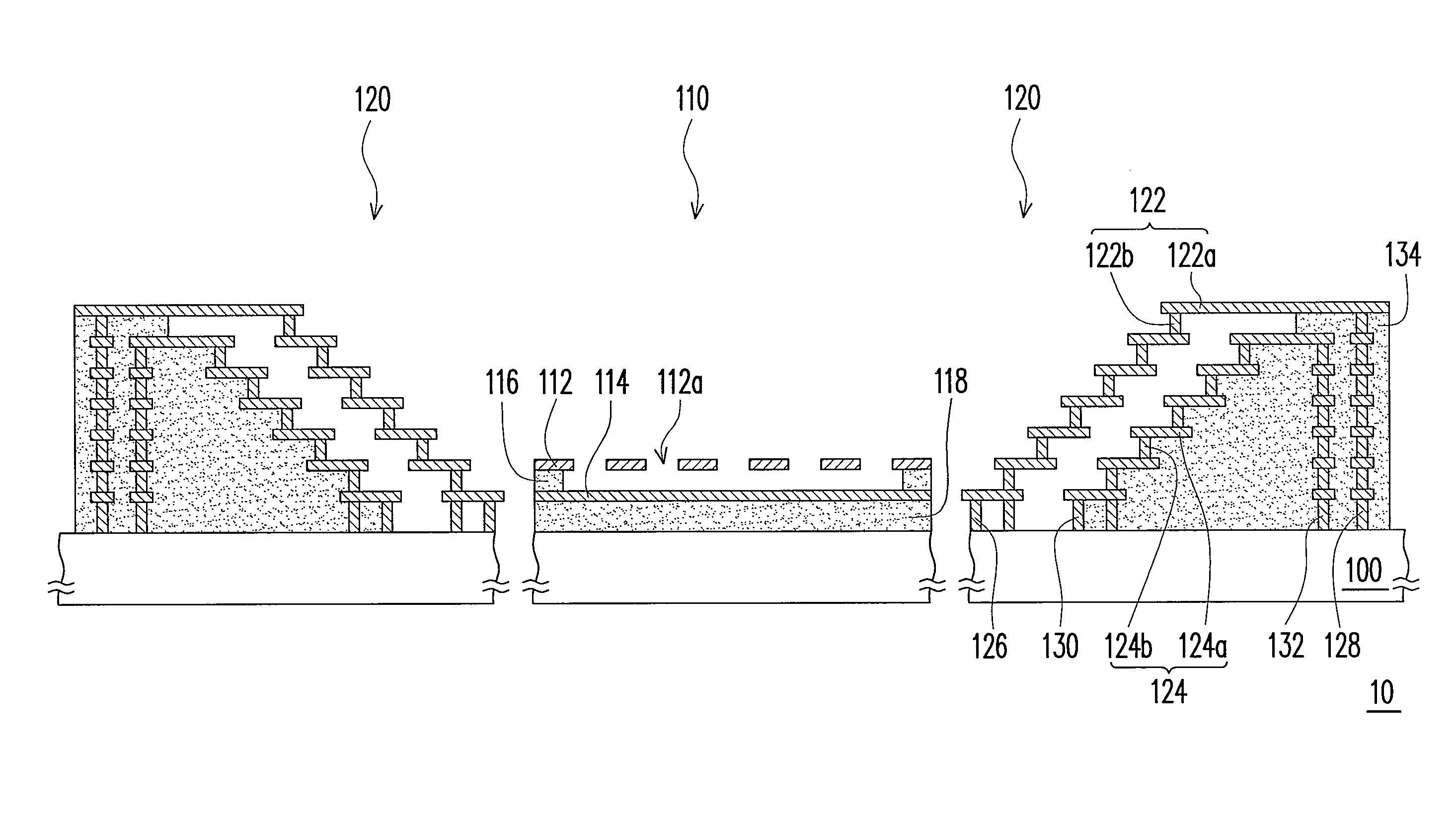
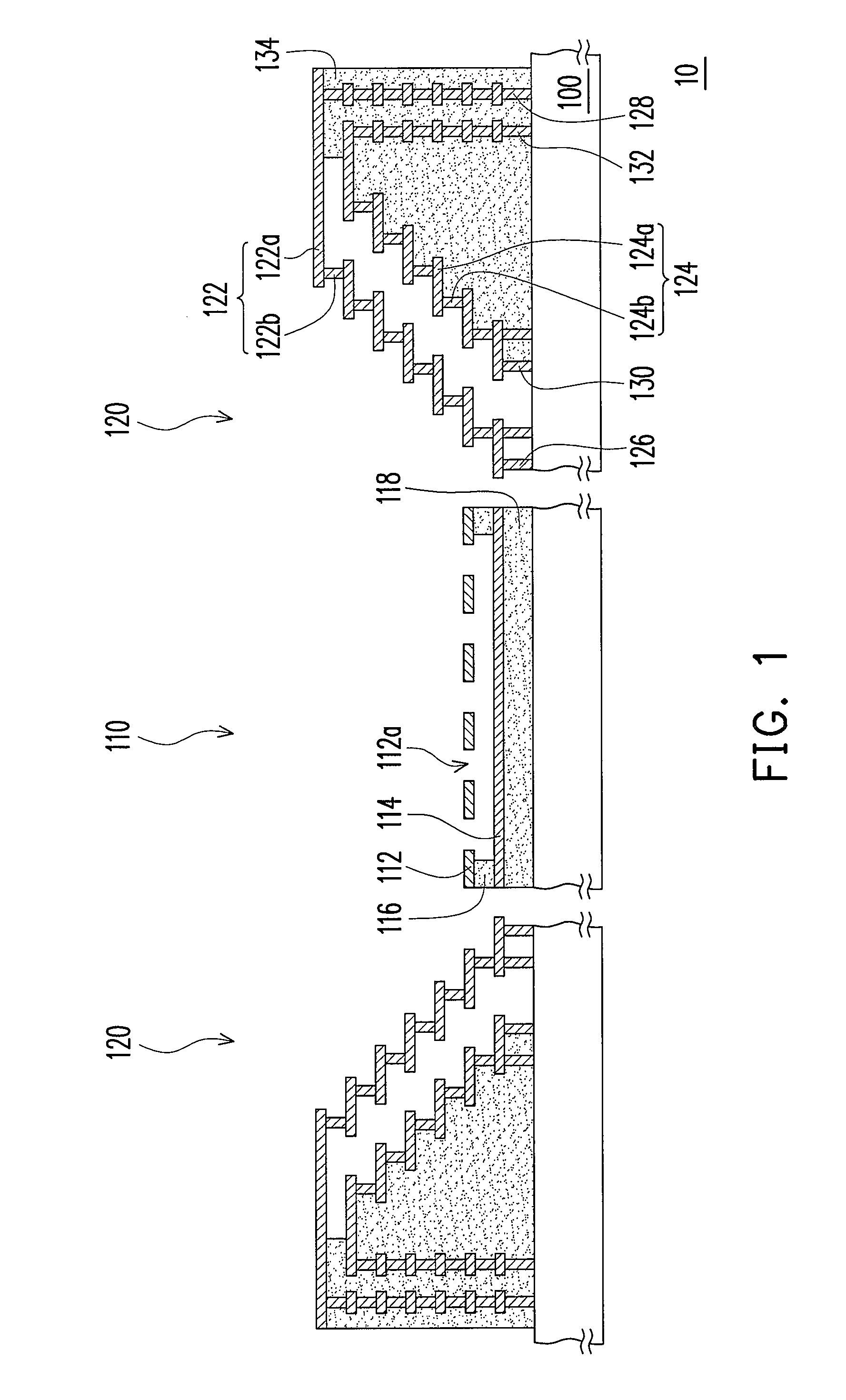
[0027]FIG. 1 is a schematic cross-sectional view of a microelectromechanical system microphone structure according to a first embodiment of the present invention.
[0028]Referring to FIG. 1, the microelectromechanical system microphone structure 10 includes a substrate 100, a first device 110, and a second device 120.
[0029]The first device 110 is disposed on the substrate 100, and includes a first upper electrode 112, a first lower electrode 114, a dielectric layer 116, and a dielectric layer 118. In this embodiment, the first upper electrode 112 includes, for example, a plurality of holes 112a. Therefore, the first upper electrode 112 is a mesh electrode, and the material thereof may be polysilicon, polysilicon metal, aluminum, tungsten, copper, titanium, or other conductive materials. The first lower electrode 114 is disposed between the first upper electrode 112 and the substrate 100, which may be, for example, a whole piece of electrode, and the material may be...
second embodiment
The Second Embodiment
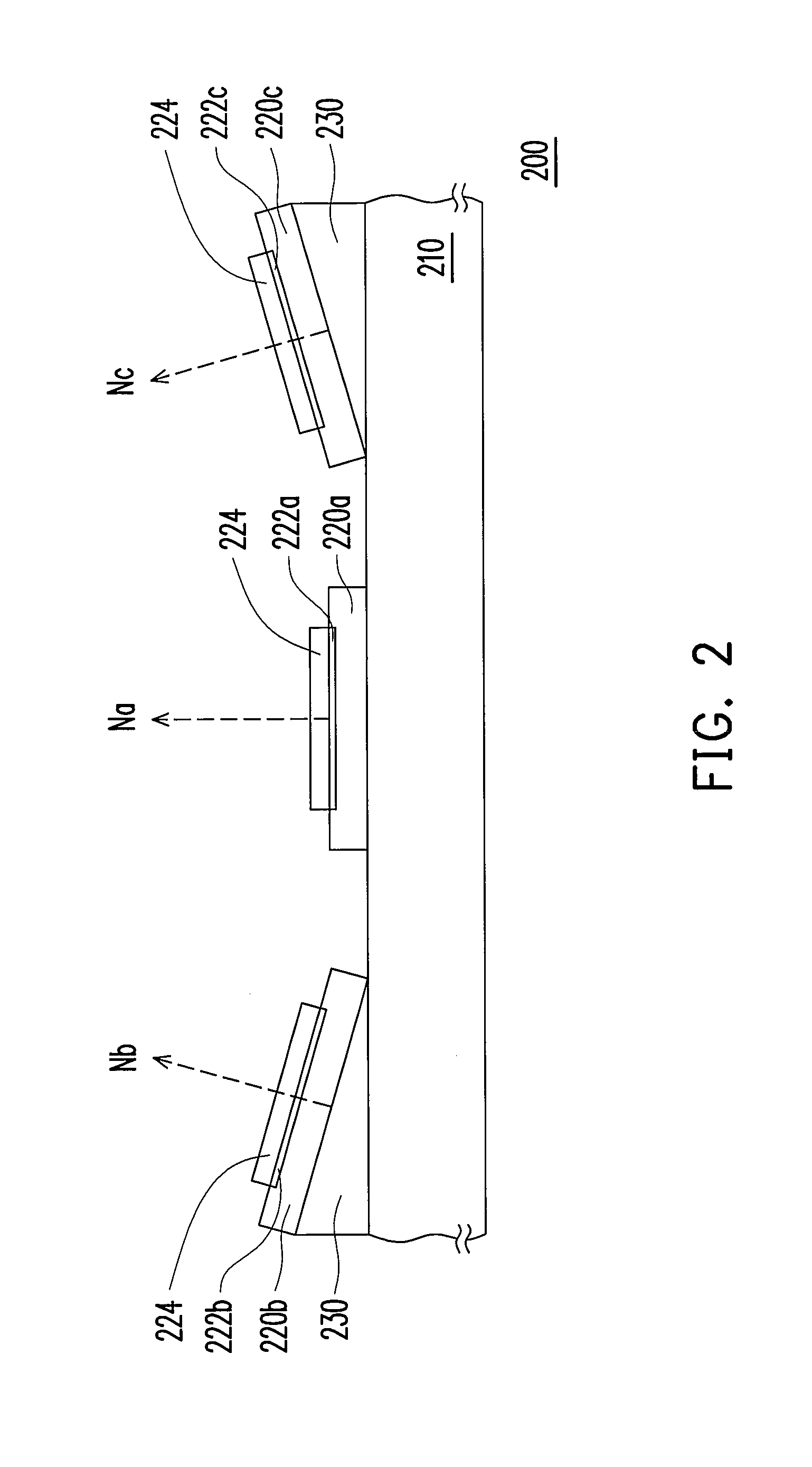
[0034]FIG. 2 is a schematic cross-sectional view of a microelectromechanical system microphone package structure according to a second embodiment of the present invention.
[0035]Referring to FIG. 2, the microelectromechanical system microphone package structure 200 includes a base plate 210, a plurality of chips 220a, 220b, and 220c, and holders 230. The chips 220a, 220b, and 220c are disposed on the base plate 210, and for example, the chip 220a is surrounded by the chips 220b and 220c.
[0036]The chips 220a, 220b, and 220c respectively have active areas 222a, 222b, and 222c, and each of the active areas 222a, 222b, and 222c is provided with a microelectromechanical system microphone structure 224. In other words, the chips 220a, 220b, and 220c are MEMS microphone chips. The structure of the microelectromechanical system microphone structure 224 may be similar to the structure of the first device 110 in the first embodiment or other structures, which is not limit...
PUM
Abstract
A microelectromechanical systemmicrophone structure including a substrate, a first device and at least one second device is provided. The first device is disposed on the substrate and including a first upper electrode and a first lower electrode disposed between the first upper electrode and the substrate. The second device is disposed on the substrate, surrounding the first device and including a second upper electrode and a second lower electrode disposed between the second upper electrode and the substrate. The second upper electrode includes a plurality of first conductive layers and first plugs. The first conductive layers are arranged in steps, and the first plug is disposed between the adjacent first conductive layers. The second lower electrode includes a plurality of second conductive layers and a plurality of second plugs. The second conductive layers are arranged in steps, and the second plug is disposed between the adjacent second conductive layers.
Description
BACKGROUND OF THE INVENTION[0001]1. Field of the Invention[0002]The present invention generally relates to a semiconductor device, in particular, to a microelectromechanical systemmicrophone structure and a microelectromechanical systemmicrophonepackage structure.[0003]2. Description of Related Art[0004]Microelectromechanical System Device (MEMS device) refers to a microelectromechanical device manufactured in a miniaturized package structure with a technology extremely similar to a technology for manufacturing an integrated circuit (IC). However, the MEMS device interacts with a surrounding environment in more manners than a conventional IC, such as interaction in mechanics, optics, or magnetic force. The MEMS device includes tiny electromechanical devices, such as an accelerometer, a switch, a capacitor, an inductor, and a microphone. The MEMS device manufactured with an MEMS technology has many advantages. For example, an MEMS microphone manufactured with the MEMS technology h...
Claims
Application Information
Patent Timeline
Application Date:The date an application was filed.
Publication Date:The date a patent or application was officially published.
First Publication Date:The earliest publication date of a patent with the same application number.
Issue Date:Publication date of the patent grant document.
PCT Entry Date:The Entry date of PCT National Phase.
Estimated Expiry Date:The statutory expiry date of a patent right according to the Patent Law, and it is the longest term of protection that the patent right can achieve without the termination of the patent right due to other reasons(Term extension factor has been taken into account ).
Invalid Date:Actual expiry date is based on effective date or publication date of legal transaction data of invalid patent.

